by Goran Panic, Zoran Stamenkovic, Klaus Tittelbach-Helmrich, Jens Lehmann, Gunter Schoof IHP GmbH Im Technologiepark 25 D-15236 Frankfurt (Oder), Germany Abstract:
In this paper we study the use of scratchpad memories in low-power embedded systems for wireless applications. As an example, we designed a general-purpose microcontroller-based system-onchip that is used as a part of an evaluation platform aimed for hardware and software development of wireless systems. The system is constructed around the AMBA platform and is based on the MIPS 4KEp embedded core that includes scratchpad memories for instructions and data.
The paper describes the scratchpad system integration, implementation and verification methodology, and also depicts the system performance at the evaluation platform for wireless applications.
1. INTRODUCTION
In the last decade, a tremendous growth has been made in the area of wireless networking and communications, where the power consumption is acknowledged to be a major merit for the overall system quality. Therefore, the power optimization techniques have become the most important design issue, and are applied at all stages of system design.
At IHP [1] we develop embedded systems for wireless applications that usually consist of a number of cores optimized for specific processing tasks. The systems are being developed around the IHP wireless engine platform (Figure 1) that specifies main parts of a wireless communication system to be integrated on a single chip. The platform presents a multiprocessor system consisting of protocol and application engines interconnected with a baseband processing unit and an analog front-end. The platform specifies a power optimization mechanism that benefits from the interlayer optimization, where the overhead introduced by complex protocol functions is reduced by introduction of dedicated hardware accelerators in the protocol cores. The embedded protocol systems usually include an embedded processor that executes a part of the protocol functionality where the protocol is stored in an embedded on-chip memory. Many embedded CPU cores available on the market, provide support for embedded scratchpad memories (SPRAMs). The SPRAMs are software controlled and have better power efficiency than caches [2]. In order to evaluate the scratchpad suitability for our applications we designed a test system-on-chip based on a MIPS 4KEp [9] core with scratchpad support.
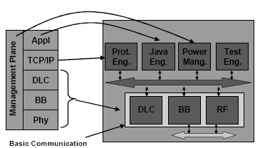
Figure 1. IHP Wireless Engine Platform
The reminder of the paper is organized as follows: Section 2 discusses the scratchpad functionality, integration options and interface to the core. The architecture of the designed test system is presented in Section 3, as well as the applied implementation and verification methodology. Section 4 describes the system performance measured on an evaluation platform. The conclusion and directions for future work are given in Section 5.
2. SCRATCHPAD MEMORIES
The term scratchpad memory usually refers to the embedded on-chip memory used to store instructions or data. Unlike the caches, the scratchpads are software controlled. They are mapped to the processor’s address space and their use is controlled by a user’s application. The main advantages of SPRAMs over caches are: 1) reduced chip area, since there’s no need for additional tag and way select memory arrays and no complex cache hit logic is present, 2) reduced power consumption, since only simple SPRAM hit logic is used, 3) flexibility, since user have full control of SPRAM access, and, 4) performance, since scratchpad access is in general faster than cache access. Disadvantage is in additional effort required to program the system based on SPRAMs. In the case of an application that significantly exceeds an available SPRAM space, the overall performance is affected by the ability of a compiler to efficiently utilize this space. At the moment, no commercial compilers are available that can efficiently perform this task. Some efforts in this direction have been made in [3,4,5]. With no compiler support, it’s up to user to decide which part of the program should be stored in SPRAM, and if and how it would be changed during execution. It is possible with the modern RISC cores to combine both the scratchpads and caches to work concurrently. In that case the user should select an optimal configuration that meets its target system requirements.
2.1. Scratchpad Integration
The integration of SPRAMs into a system mainly depends on the specific system’s architecture and the target application. Nowadays, many commercially available RISC CPU cores have an option to include SPRAMs. For example, common configurations for 803x/805x compatible 8-bit microcontrollers allow integration of maximum 256 bytes of internal data SPRAM (DSPRAM) and up to 64 KB of internal ROM (Synopsys dw_8051) [8]. The more advanced 68HC11 compatible 8-bit microcontrollers allow integration of maximum 1024 bytes of DSPRAM and up to 64KB of internal ROM (Synopsys dw_6811) [8]. In the case of highperformance 32-bit RISC processors, both data and instruction scratchpads (ISPRAM) are supported as well as concurrent cache integration. There are many embedded CPU vendors offering a variety of core architectures with scratchpad support that can answer to almost any customer demand. Some of them, offered by ARM [6] and MIPS [7], are listed in Table 1. Note that ARM uses the term TCM (Tightly Coupled Memory) to refer the scratchpads.
| ARM 968E-S | MIPS 4KEp | ARM 1026EJ-S | MIPS 24KE | ARM 1136JF-S |
| Pipeline | 5-St. | 5-St. | 6-St. | 8-St. | 8-St. |
| Cache | / | 64KB | 128KB | 64KB | 64KB |
| ISP | 4MB | 1MB | 1MB | / | 64KB |
| DSP | 4MB | 1MB | 1MB | 64KB | 64KB |
Table 1. Memory options for different types of commercially available 32-bit microcontrollers
The high-end embedded RISC cores usually provide customizable SPRAM ports that act as simple memory-like interfaces. Usually, there are separate interfaces to data and instruction SPRAM that user needs to customize to fit the target memory device. We will describe the features of SPRAM interface on the example of MIPS 4KEp [9] embedded core but the main ideas are general and can be found in similar forms at other vendor’s cores.
2.2. Scratchpad Interface
The SPRAM interface (Figure 2) on a MIPS 4KEp core is designed to provide low-latency access to on-chip memories. The SPRAM port is accessed in parallel with the caches. This saves a number of cycles that would normally be required going through the bus interface unit and the EC interface. The SPRAM array effectively replaces a cache way and is always located at the last cache way. If caches are present in conjunction with SPRAM, then the maximum cache associativity is 3. A full tag array is not needed for SPRAM since, equivalent tag functionality is achieved by a simple decode of the physical address to determine hit or miss. The cache way-select array is not needed for SPRAM.
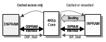
Figure 2. SPRAM interface on 4KEp
The 4KEp core provides separate interfaces for ISPRAM and DSPRAM which presence can be independently configured. A SPRAM array can be up to 1MB in size. The ISPRAM can service uncached references, enabling processor boot with no EC interface accesses. The SPRAM port can stall the core if the SPRAM array was busy the previous cycle or if data is not ready. This can enable other sources to access the SPRAM without the need for dual-porting the array. This is useful, for example, if there is a DMA engine filling the
SPRAM or if a unified I/D SPRAM is desired. A cache, in contrast, has fixed single-cycle timing.
The SPRAM interface is designed to be flexible enough to work with a variety of system designs. A variety of memory devices can be connected to the SPRAM interface: SRAM, ROM, flash, etc. If desired, memory-mapped functions can also be connected, as long as the interface protocol is met. Multi-ported devices can also be used; in this case, the ISPRAM or DSPRAM interface is logically connected to just one of the ports, with other system logic unrelated to the 4KEp core utilizing the other port(s).
3. DESIGN OF A SCRATCHPAD BASED SOC
In order to evaluate the scratchpad applicability for our systems we designed a test chip containing an embedded CPU with the scratchpad support. The chip contains no application-specific logic and is the very first step in designing complex wireless systems.
3.1. System Architecture
The system architecture is presented in Figure 3. The system is based on MIPS 4KEp core [9] connected through the AMBA bus [10] to system peripherals. The core integrates both instruction and data scratchpad memories with sizes of 8 Kbytes each. A memory controller is attached to the AMBA advanced high performance bus (AHB). It provides an interface to an external Flash memory and static RAMs. The slower AMBA advanced peripheral bus (APB) is attached to AHB via AHBto- APB Bridge. Two UARTs and GPIO are connected to APB.
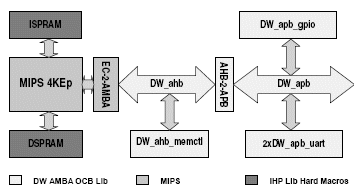
Figure 3. System architecture
3.1.1. IP cores.
Most of the components used in the design are taken from the Synopsys DesignWare AMBA On-Chip Bus library [8]. The DesignWare AMBA OCB provides synthesizable components and verification models in a technologyindependent bus system that one can configure with an easy-to-use tool interface. The CoreConsultant tool [11] is used for components configuration, verification and synthesis. The components in the Synopsys library are firm IP components delivered in a form of encrypted Verilog integrated into configurable core kits. The processor core is purchased as a soft core from MIPS. The delivery includes a GUI for core configuration and a number of scripts for core synthesis and verification. The bridge for connecting the processor to an AMBA bus comes from MIPS as well. It is configured according to application-specific demands and synthesized using delivered scripts. Finally, the memory blocks are introduced in the layout stage as hard macros.
3.1.2. System Planning.
Before the particular components are configured, it is required to plan the system architecture and to define the correct memory mapping. Defining the memory space is directly related to the address space of the target processor. It must be considered that the address space has to be reserved for SPRAMs, too.
3.1.3. Processor Core.
The 4KEp core used in our implementation is a high-performance, low-power, 32-bit MIPS RISC core designed for custom system-on-silicon applications. It implements the MIPS32 architecture and contains all MIPS II instructions. An optional enhanced JTAG (EJTAG) block is included that allows single-stepping of the processor as well as instruction and data virtual address breakpoints. The core was configured to include 8kB of instruction and 8kB of data scratchpad memory. Two interfaces for SPRAMs are designed and synthesized separately. Each interface contains decode and hit logic for SPRAMs. Interface to AMBA bus is provided via EC-to-AMBA bridge logic. The core implements clock-gating in order to save energy.
3.1.4. AMBA AHB Bus.
DesignWare AMBA AHB Bus component (DW_ahb) is configured to include one master (Lite version) and three slaves. The first slave is a memory controller (DW_ahb_memctl), the second is a peripheral bus controller (DW_apb) and the third is reserved for the memory controller’s register file. The interface of the register file is aliased to memory controller’s interface since the register file is a part of DW_memctl. A slave in AHB can be mapped to more memory regions. In our case both the memory controller and the APB are mapped to two separate memory regions.
3.1.5. AMBA APB Bus.
DW_apb component is configured to connect three slaves: two UARTs (DW_apb_uart) and a general purpose I/O (DW_apb_gpio). UARTs and GPIO are mapped to different memory regions. The AHB-to-APB Bridge is a part of this component.
3.1.6. Memory Controller.
DW_ahb_memctl is configured to act as a static memory controller. In general, it can be configured to control both synchronous DRAMs (SDR-SDRAM, DDRSDRAM, Mobile-SDRAM and the Micron SyncFLASH) and static memories (SRAMs, FLASHes and ROMs). In our system there are three memory ports: two reserved for external SRAMs addressing the 8MB of the memory space each, and one of 16MB reserved for external boot FLASH. Three sets of registers are provided to define memory access times. These registers are assigned to every of the memory ports and default values are specified.
3.1.7. UARTs.
Two UARTs are provided in the system as an interface to external peripherals. The configuration is standard with 16 bytes wide internal FIFO. Functionality of DW_apb_uart is based on the industry standard 16550 and supports Auto Flow Control Mode (16570 compatible).
3.1.8. GPIO.
The target configuration of GPIO includes a single 32-bit port. DW_apb_gpio supports up to 128 independently configurable pins. The pins are distributed in four separately configurable ports, with configurable hardware and software control for each port.
3.2. System Implementation and Verification
The used design flow is typical for the design reuse methodology. Considering the defined system architecture, the reusable components are configured and the custom logic is designed and verified as well as the top-design.
3.2.1. Synthesis.
The most of the components are automatically synthesized and verified after a component’s configuration is chosen. As a result, the library-mapped and generic netlists are generated. The synthesis is performed with Synopsys Design Compiler tool [12] for the target frequency of 80 MHz using the worst-case libraries.
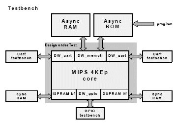
Figure 4. Testbench block diagram
3.2.2. Verification.
The verification process includes verification of standalone IPs and verification of complete system. The particular components are verified within the corresponding configuration environments before and after they have been synthesized. Since the verification of single components does not guaranty correctness of the complete system, a simulation environment with a standalone testbench is created for it’s testing (Figure 4).
The testbench uses HDL verification models attached to the external interfaces of the system and behavioral simulation models for SPRAMs and external memories. We have written a generic assembly program to be stored in the simulation model of the boot flash. The program includes processor initialization phase, a boot loader for copying of test programs to ISPRAM and test program itself. After reset is released, a test program is copied to ISPRAM, read from it and executed. A number of test programs were written in order to test as many features of the chip. The tests perform various transactions on each of the system ports and test specific operations of the chip. The same tests are used to verify RTL model of the chip, synthesized gate-level netlist and after-layout netlist.
3.2.3. Layout.
After functionality of the synthesized design is verified, the layout of the chip is designed. The Cadence SoC Encounter tool [13] is used. The system is produced in IHP 0.25mm CMOS technology and tested with the Agilent 93000 chip tester. The die photo is shown in Figure 5.
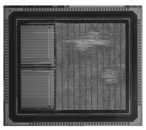
Figure 5. Die photo
Table 2. Summarized features of the chip
| Size | 20.6 mm2 |
| Number of ports | 119 signal + 16 power |
| Max operating frequency | 100 MHz |
| Power consumption | 280mW@2.5V, 90MHz |
| Number of transistors | ~1.600.000 |
The features of the chip are summarized in Table 2. The data show that the high-performance of the system is reached along with a significant reduction of power consumption.
4. SYSTEM PERFORMANCE
To verify our approach, we compare the features of functionally equivalent systems based on scratchpads and caches. Also, the system performance is evaluated at a hardware platform designed for developing and testing of wireless applications and systems.
4.1. Scratchpad-based vs. Cache-based System
Prior to hardware analysis of our test system we performed theoretical analysis and comparison between two processor’s configurations, one having scratchpad memories and another having directmapped caches of same size. The estimated area and power consumption of implemented processor configurations are compared in Table 3.
Table 3. Features of the processor configurations
| SPRAM-based | Cache-based |
| Area | 6.5 mm2 | 8.2 mm2 |
| Power Consumpt. (2.5V and 80MHz) | 250 mW | 330 mW |
| Max. Frequency | 90 MHz | 85 MHz |
As it was expected, the core having caches has significant increase in logic area compared to the SPRAM-based one. Additionally, the cache-based core includes additional memory arrays for tag and way select fields, making the difference even larger. The power estimation is performed with Synopsys PrimePower tool [14] using custom applications to be executed from the cache, and respectively from the ISPRAM. In most cases the analysis has shown significantly lower power consumption of the SPRAM-based configuration.
4.2. Evaluation Platform
In general, the evaluation of SoCs designed at IHP is performed on the hardware platform we have designed for the purpose of system development and testing (Figure 6). The platform consists of one or more mutually interconnected subsystems. Each subsystem contains the printed circuit board controlled by a workstation containing the socket for a daughter board. The chip under evaluation is assembled on the daughter board (Figure 7). The subsystems are connected via the link emulator board containing a FPGA that can be programmed for a specific application. The main board contains SRAM and FLASH memories, voltage and clock regulation circuitry, LED display, connectors to the probes from signal analyzer and EJTAG connector to MIPS hardware debugger.
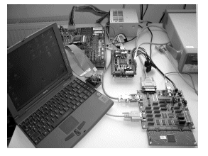
Figure 6. IHP Evaluation Platform
Additionally, there are two serial and one parallel connector for connection to a PC and the link emulator. The functioning of the complete system is controlled via debug monitor program, which was internally developed. In the case that the chip under evaluation contains some specific interface like PCMCIA, the corresponding connectors can be inserted on a daughter board enabling the workstation to access it.
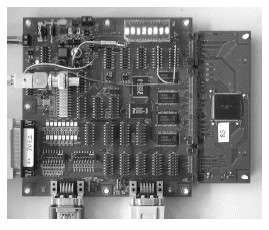
Figure 7. The test chip on the daughter board connected to the main board
The fabricated test chip is extensively tested for functionality using our evaluation platform. We developed routines that enable the monitor program on a workstation to efficiently change the content of ISPRAM. A number of applications are executed from the ISPRAM and the performance and power consumption is measured. The measurements show high performance, with significantly lower power consumption, compared to the equivalent cachebased systems we have designed in past.
5. CONCLUSIONS AND FUTURE WORK
We have demonstrated a methodology to design systems for wireless applications based on an embedded processor with the scratchpad support. The test chip is designed as well as an evaluation platform in order to evaluate the presented concept. The main advantages of the systems containing embedded SPRAMs over the cache-based are in decreased power consumption and reduced area of the chip. However, an additional effort is required to develop the software that efficiently utilizes the system resources.
Using presented methodology we have already designed the prototypes of some protocol systems used in WLAN (IEEE 802.11a MAC, TCP/IP, encryption cores, etc.). Using the evaluation platform we were able to connect two subsystems to communicate over the link emulator. The system is shown to be very useful for software and hardware debugging and testing of newly added features.
In the future we plan to make systems with a higher level of integration where more subsystems and additional features should be integrated on a single chip. For the systems running at low frequency, like sensor networks nodes, we plan to insert FLASHbased SPRAM that has much better area utilization than SRAM.
6. REFERENCES
[1] IHP GmbH, (http://www.ihpmicroelectronics.com)
[2] R. Banakar, S. Steinke, Bo-S. Lee, M. Balakrishnan, and P. Marwedel, Scratchpad Memory: A Design Alternative for Cache On-chip memory in Embedded Systems, CODES, Estes Park (Colorado), May 2002.
[3] M. Kandemir, J. Ramanujam, M. J. Irwin, N. Vijaykrishnan, I. Kadayif, and A. Parikh, Dynamic Management of Scratch-Pad Memory Space, Proc. of 38th Design Automation Conference, pages 690– 695, Las Vegas, NV, Jun 2001.
[4] M. Kandemir, I. M. Vijakrishnan N., and W. Ye. Influence of compiler optimizations on system power, Proc. of the 37th Design Automation Conference, pages 304–307, Los Angeles, CA, Jun 2000.
[5] Stefan Steinke, Lars Wehmeyer, Bo-Sik Lee, Peter Marwedel, Assigning Program and Data Objects to Scratchpad for Energy Reduction, DATE 2002, Paris/France, March 2002.
[6] ARM Inc
[7] MIPS Technologies
[8] Synopsys DesignWare® Library, Synopsys inc.
[9] MIPS32TM 4KETM core family, MIPS Technologies
[10] AMBA On-Chip Bus Standard, ARM Inc,
[11] CoreTools, Synopsys Inc,
[12] Design Compiler, Synopsys Inc
[13] SoC Encounter, Cadence Inc
[14] PrimePower, Synopsys Inc