W.J.Bainbridge, A.Bardsley, R.W.McGuffin Silistix Ltd, Manchester, UK Abstract
The CHAIN NoC combines the architectural benefits of a networking approach over a conventional bus hieraarchy, with the timing closure and power-management benefits of self-timed design. The result is a flexible, clockindependent solution to the complexity, power-management and timing closure problems of SoC interconnect in deep submicron VLSI systems.
This paper introduces the basic CHAIN architecture using a small test-chip as an example application. It then presents the CHAINworks library and toolset which supports the development of self-timed Networks-on-Chip using industry accepted design and tool flows.
1. Introduction
The interconnection of the many components of a system- on-chip (SoC) is becoming increasingly difficult as systems become more complex and the relative delay cost of wires over gates becomes more significant with every CMOS feature size shrink.
Currently, designers use an ad-hoc hierarchy of clocked system buses interconnected by bridges as illustrated in Figure 1. The desired clock frequencies of these buses are chosen based upon the communication needs of the devices connected by the bus. However, the actual achieved frequencies are limited by the physical length of the bus wires and by the amount of design time that can be spent on optimising the physical layout of the SoC.
The design complexity of bus-hierarchy based system is becoming intractable. In an analogous move of the telephone system from circuit switching to packet switching, it is apparent that a move from the current bus-hierarchy based approach to one using networking techniques is the only viable solution to the complexity problem. It is argued here that a self-timed implementation of networks-on-chip is the only viable solution to the timing closure and power management problems associated with such complex implementations.
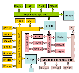
Figure 1
Systems built around a self-timed NoC such as the Silistix CHAIN NoC allow the globally asynchronous connectivity of IP blocks each operating at their own frequency (with either synchronous or self-timed implementations), resulting in a globally-asynchronous, locally-synchronous (GALS) system, as recognised by the ITRS roadmap.
2. The CHAIN Architecture
CHAIN [4] is an approach to SoC interconnect using a network of low-cost switches and narrow links all operating using delay-insensitive self-timed protocols. The links and switches, which can be ganged together for increased throughput, are then used in conjunction with well-defined packet formats to provide virtual connections between client devices.
2.1. Self-timed link protocol
The individual CHAINlinks, illustrated in Figure 2, comprise five forward-going signals and an explicit acknowledge signal to allow self-timed flow control. The data-encoding used on these links is a 1-hot code allowing either 2-bits of data or a control marker, end-of-packet (eop), to be sent on each communication. A return-to-zero protocol is used so that after each communication, the link returns to the idle state. There are, therefore, four signal transitions (two data, two acknowledge) for every two-bit communication.
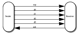
Figure 2: CHAIN link
2.2. Scalable performance
The significant delays incurred due to long wires on small feature-size CMOS processes mean that repeater stages are often required to repower the signal, resulting in propagation delays proportional to the connection length.
With the CHAIN NoC, these repeaters are replaced with pipeline latches, allowing the cycle-rate of the links to be increased, whilst adding little additional latency over that of a simple repeater. This type of change exploits one of the benefits of the self-timed implementation style where the pipelining depth can be varied with little effect on latency, unlike the synchronous design style where every extra pipeline stage adds another clock period of latency. As a result, each link in the network can be tuned separately, as the interconnect is no longer restricted by a (slow) global clock limiting the fabric’s performance. A suitable CHAIN pipeline latch implementation is shown in Figure 3. The key features in this circuit are the datapath latches (actually Muller C-elements [6], similar to transparent latches) and the OR-gate detecting the presence of a valid, latched output and generating an input-acknowledge.
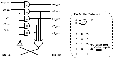
Figure 3: CHAIN pipeline latch
The variation in the cycle-rate of a CHAIN link stage for different link lengths, based on SPICE RC-network simulations for a TSMC 180nm CMOS process with aluminium wires, is shown in Figure 4. For a 2mm link, it can be seen that the cycle-rate is ~380MHz, giving a throughput of about 0.75Gb/s/link. For higher throughputs, links can be ganged together to form a wider datapath. It should be noted that the repeaters used were only x2 standard drive cells. The 2mm link cycle-rate can be improved to ~500MHz using cells with stronger outputs.
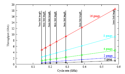
Figure 4: CHAINlink cycle-rate v length
2.3. Packet switching
The pipeline latch/repeater shown in Figure 3 can be extended [4], to form the basic modules of a switched network- on-chip. The CHAIN NoC uses a distributed switching fabric, where the data transported between the network gateways is passed in messages formatted as packets each beginning with a route used to steer the packet along a path to the receiver gateway, and ending with an end-of-packet marker to allow clear-down of such paths once the packet has passed. The packet format used in the network for the ‘Buxton’ test chip [3] is:
- Route symbols transmitted at the start of the packet
- An 8-bit packet header containing a sequence-tag and initiator-identifier for the transaction
- An 8-bit bus-message header carrying bus-control signals and describing the type of bus-transfer data carried in the payload
- A payload split into a number of 16-bit chunks
- An end-of-packet marker
Where a connection in a network uses a gang of links as described above, the route and end-of-packet symbols are replicated on all of the links in the gang, and the packet body (the messages) is spread across the links in the gang. This strategy, used in our test-chip is one of many that can be applied when using ganged links, examples of others including spreading the route across the links, rather than replicating it, or transmitting route/eop information on only one link, with the other ganged links being switched in the same manner as this link in a master/slave relationship
3. Network gateways and interface adapters
At the endpoints of the network fabric are the network gateways which perform the many control functions and data-formatting operations necessary for message exchanges across the switched network fabric. These include:
- serialisation/deserialisation to allow ‘parallel’ data to be transmitted across the narrow connections of the network fabric;
- determining the routing symbols required to steer a packet from the sender to the receiver and transmitting these at the start of the packet;
- constructing and processing the message header showing the packet and payload type;
- transmitting the end-of-packet symbol after the last part of the message to clear-down the network path transmitted by the packet;
- flow control to minimise congestion of the network fabric or gateway receive buffers.
Gateways typically have two ports into the network, one for sending packets and one for receiving. Dependent on the topology of the network fabric, such gateways may provide initiator and/or target capabilities for their connected client IP core or bus-based client IP subsystem.
The internal structure of an initiator gateway as used in the test chip is shown in Figure 5.
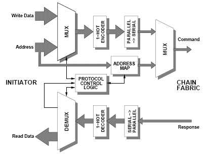
Figure 5: Initiator gateway
The Silistix network gateways speak a proprietary socket format operating with a self-timed protocol, known as the CHAIN Gateway Protocol (CGP), and hence support and facilitiate the reuse of existing IP-blocks constructed with the interfaces of today’s defacto bus standards (AMBA[1], OCP, CoreConnect[2]) through a library of client adapters for mapping between the CGP socket and the legacy protocols. In addition to mapping bus concepts onto networking functions, these adapters handle bus transaction ordering issues and conversion between the self-timed CGP socket and the synchronous nature of the legacy bus protocols.
4. Test-chip network
Much of the NoC technology described here has been implemented in a 180nm CMOS process from TSMC on the ‘Buxton’ smartcard test-chip [3] created by the University of Manchester. The network for that system had three initiator gateways, 6 target gateways and a network debugging port allowing direct access to the fabric from off-chip. The network had two separate segments, the first carrying commands from the initiators to the targets, and the second carrying responses back to the initiators.
4.1. The network fabric
Since the required performance of the smartcard system was only 10 MIPS, there was no need for a complex, highperformance network in this system. This allowed exploitation of the low-end of CHAIN’s scalability in three areas:
- Link-length - low performance requirements allowed links of around 2mm to be used giving around 0.75Gb/s throughput per link.
- Gang width - a gang of two links gives an aggregate throughput of 1.5Gb/s, which gives an upper bound on message throughput of about 31 million messages/second (for a 48-bit read-command/read response message) and a fabric-imposed latency of 32ns over-and-above the route-setup time.
- Topology - minimal concurrency was required since the two processors would not (in normal circumstances) be simultaneously enabled, and did not support memorysystem pipelining. A simple concentrate/expand topology, analogous to a shared bus, was adequate.
This meant that the fabric was composed of connections formed from two outgoing links to carry the commands, and two returning links to carry the responses with the switching components connected as shown in Figure 6.
4.2. Network gateway adapters
The test-chip had two (self-timed) microprocessors and a test-interface as the initiators and a variety of memories plus a UART and an experimental unit as the target. The
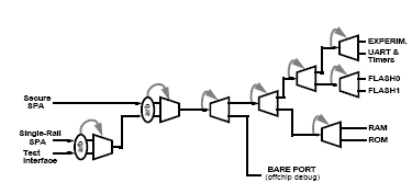
Figure 6: Network fabric composition
processors required very little interface adaption for connection to the CGP socket, small adapter wrappers were required for the other devices.
4.3. Component placement
The final layout of the chip is shown in Figure 7 with the CHAIN links and the fabric switches highlighted. The only constraint on the floorplanning stage was to roughly balance the lengths of the CHAIN links, keeping the long links below 2mm. This was not difficult.
4.4. Design validation and timing closure
The system was extensively simulated using extracted transistor/capacitance netlists of the two processors, functional models for the memories and basic, non-extracted transistor netlists (no RC values) for the CHAIN network. The goal was to validate the functionality and correct timing behaviour of the computational blocks.
The CHAIN network fabric was not extracted prior to device fabrication, since the self-timed design guarantees correct-by-construction timing behaviour and the network offered a significant margin over the required system performance level.
With the fine-grained control over the network performance provided by the ability to choose arbitrary link-lengths and gang-widths as described earlier, system-level interconnect timing validation should be much simpler (and shorter) in the majority of systems built around CHAIN where sufficient margins can be designed in. Although designs will always function correctly, in extremely high performance systems, some simulation will still be desirable to validate the network performance.
4.5. Tool flow
The design of the network and creation of the necessary components for this test-chip were both manual processes. The remainder of the flow used conventional, commercially available EDA tools from Synopsys and Cadence for structural simulation, static timing analysis, layout, extraction and transistor-level simulation. A conventional standard cell library augmented with a small number of special self-timed cells (a Mutex [after 7] and Muller C-elements [6]) was used. Although these cells can be constructed from conventional synchronous cells, they were designed as custom primitives to improve performance and reduce area penalties.
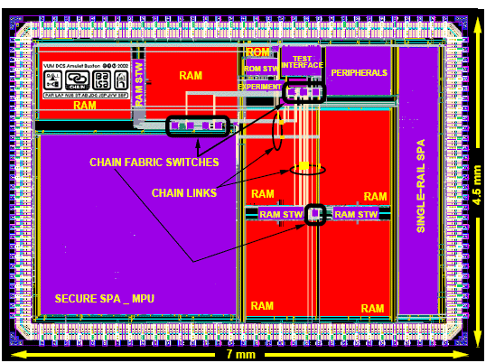
Figure 7: The Buxton smartcard chip
4.6. Measurements and results
One of the network targets had additional logic to aid debug and measurement of the the network’s performance. Further details on the debugging of this chip and the support provided by the CHAIN network can be found elsewhere [5].
It was confirmed that the CHAIN fabric did in fact operate at just over the nominal 500MHz cycle-rate predicted by simulations, illustrated in Figure 4, for the longest link on the chip which is about 1.5mm in length. As noted earlier, these links all suffered from weak drivers and should be able to operate faster if correct signal buffering is applied. Power measurements were not attempted since there was no equivalent synchronous system for comparison; also power dissipation would be determined by activity which, in turn, would be determined by the system software.
5. The CHAINworks: commercial CHAIN NoC deployment
The networks used for the smartcard chip described here were designed and entered manually through a schematic capture process by an expert in self-timed design. Furthermore, only a small range of architectural options were considered. This approach is inadequate for commercial use of the CHAIN network by synchronous SoC designers. Silistix, a venture funded spinout from the University of Manchester in the UK, is developing IP libraries and software tools to automate the exploration of the architectural tradeoffs possible and compile the chosen network. With this approach, the combined benefits of the networking approach and the self-timed implementation are provided without the synchronous SoC integrator having to understand these complex areas of design.
The following sections outline, in summary form, the CHAINworks components.
5.1. Requirements input
CHAINworks takes input in the form of a SystemVerilog structural representation of the network’s ports for connecting clients, or as a block-based schematic from tools such as Mentor Graphic’s Design Architect or Cadence Composer. A bus module on this structural representation has a port for each connected client, and each port is associated with an adapter unit that provides the necessary logic to allow components using today’s defacto ‘standard’ bus interfaces such as AMBA to be connected. The network module and the adapters are all annotated with constraints to identify the connectivity requirements, e.g. the throughput between different clients, the traffic profile for a client, the interface data-bus width, the client clock frequency etc.
5.2. Design exploration
Based upon the interface requirements and the connectivity constraints provided by the user, CHAINworks allows interactive exploration of the many possible architectural trade-offs. These include changes in topology, changes in pipelining depth, link-width, etc. These architectural trade-offs manifest themselves as trade-offs in area, power, performance and validation-time of the network. Simulation of behavioural bus models with patterned traffic provides feedback to this tradeoff process. Much of this trade-off can be made before progressing further through the design flow, thus allowing greater designer efficiency as fewer iterations of the timing closure loop are required for the interconnect.
5.3. Output and flow integration
CHAINworks is designed to be integrated directly with existing design flows, and leverages existing language standards to this effect. The input is (currently) provided using structural SystmVerilog with annotations indicating the constraints. The primary output is Verilog 1995 compliant structural verilog. A number of other supplemental outputs are also provided for use further down the design flow. These include:
- behavioural models for system simulation in both Verilog and System-C;
- timing constraints (SDC format) for the place-and-route and timing analysis of the network components;
- test patterns for the manufacturing test of the network.
The position of CHAINworks within the design flow is shown in Figure 8. This also shows the forward and reverse interactions of CHAINworks with the design flow, and how it fits in the timing closure loop.
5.4. CHAINworks functionality
CHAINworks comprises three key components, surrounded by netlisting and design capture. These three parts are Jaquard, Fitter and Handloom.
The synthesis approach adopted by CHAINworks is based upon the compilation of larger modules from small hardware templates, the internal flow being shown in the right half of Figure 8. The templates in the library range from fragments of circuits, through pipeline stages, switches and serialisers, to entire network gateways. These library components are all implemented using self-timed techniques, and are highly parameterized across datawidths, encodings and speed.
The choice of which components to use, and how to connect them is made by the ‘Fitter’ constraint solving part of the CHAINworks flow, guided by the user through the Jaquard visualisation support module. Once a satisfactory ‘design’ is achieved, the CHAINworks backend, ‘Handloom’ performs technology mapping to create the final structural implementation.
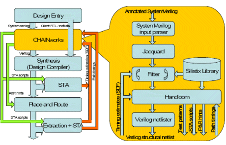
Figure 8: Silistix CHAINworks in-place in the design flow
6. Conclusions
We have shown how a self-timed network-on-chip has been successfully deployed in a system-on-chip design. The self-timed nature of the interconnect meant that there was no need to perform post-layout timing validation of the network after the final stages of system integration.
A further advantage from the self-timed operation was the ability to use only a very thin network fabric operating at a much higher cycle rate than the processing and memory subsystems that were connected, without having to provide (and timing validate) a high-speed clock.
The fabricated chip has demonstrated how a self-timed network-on-chip can perform all of the functions offered by a more conventional system bus such as allowing test access and debugging of the IP blocks within the system, whilst giving the significant advantages of self-timed operation, rapid timing closure and greater design flexibility/ scalable performance.
The technology presented here is encapsulated in the Silistix CHAINworks design tool for constructing such onchip networks.
7. References
[1] ARM Ltd. AMBA, Advanced Microcontroller Bus Architecture Specification, Rev 2.0, May 1999.
[2] IBM Corporation, CoreConnect Bus Architecture, product brief.
[3] L.A. Plana, P.A. Riocreux, W.J. Bainbridge, A. Bardsley, S. Temple, J.D. Garside and Z.C. Yu, “SPA - a Secure Amulet Core for Smartcard Applications,” Microprocessors and Microsystems, vol. 27, no. 9, Oct. 2003, pp. 431-446.
[4] W.J. Bainbridge and S. Furber, “Chain: a Delay-Insensitive Chip Area Interconnect,” IEEE Micro, vol. 22, no. 5, Sep./ Oct. 2002, pp. 16-23.
[5] W.J.Bainbridge, L.A.Plana & S.B.Furber, The Design and Test of a Smartcard Chip using a CHAIN self-timed network- on-chip, Proc DATE'04, Vol 3 pp274, Paris, Feb 2004
[6] M. Shams, J.C. Ebergen and M.I. Elmasry, “Modelling and comparing CMOS implementations of the C-element,” IEEE Transactions on VLSI Systems, vol. 6, no. 4, Dec. 1998, pp. 563-567.
[7] C.L. Seitz, System timing, in C.A. Mead and L.A. Conway, editors, Introduction to VLSI Systems, chapter 7, Addison- Wesley, 1980..