Krishnan Srinivasan, Sonics Inc
Erno Salminen, Tampere University of Technology
reprinted with permission by OCP-IP - (C) Copyright OCP-IP ABSTRACT
Performance analysis of Network-on-Chip (NoC) architectures has traditionally been done by assuming dumb slaves that return responses either immediately or with a fixed delay. Typical System-on-Chip architectures incorporating a NoC have high bandwidth communication to an external DRAM. In effect, the DRAM creates the performance bottleneck of the system. Correspondingly, performance analysis results that are presented without incorporating the DRAM controller and DRAM characteristics are likely to be overly simplistic and optimistic. Decisions that are made based on dumb slaves may lead to serious implications and system re-architecture late in the design cycle when actual DRAM memories fail to deliver the expected performance.
Creating a DRAM model for performance analysis may also not be very practical due to the sheer complexity of the DRAM controllers, and the need to adapt to newer DRAM technologies as they emerge. This paper provides a set of necessary parameters that can be used to generate a highly abstracted DRAM controller and memory. The objective is to keep the abstraction level high enough to make development easy, and at the same time, capture the critical parameters that significantly influence the performance of the system. The values of the parameters can be obtained from the JEDEC standards for the desired DRAM memory. Based on these values, the memory model can inject transaction specific latencies. This model is expected to help system architects get a more realistic picture of their system and thus help design the NoC as part of the system as opposed to treating the NoC in isolation.
1. Introduction
In the past few years, performance analysis of System-on-Chip (SoC) incorporating NoC has attracted considerable attention [1]. The OCP-IP working group has a dedicated group of members that work on performance analysis strategies for the NoC [2]. Work such as [3] and [4] have emerged out of this initiative. Traditionally, performance analysis of the NoC has been done with focus only on the NoC and in many cases, with unidirectional transmissions (load-latency) and quite often with uniform spatial distribution [5]. Alternatively, many analysis frameworks assume that a set of master transactors issue requests to a set of slaves, and the slaves return responses with zero or a fixed latency. However, such performance analyses have clear limitations.
In many MpSoC (Multiprocessor SoC) architectures, several masters communicate with a single or at most few DRAM (dynamic RAM) memory slaves, see [7] for examples. Figure 1 shows an example architecture where processing elements (PEs) are interconnected with a 2-D mesh network. A Network interface (NI) is placed between PE and network router. A highly utilized external memory is problematic because the large fraction of the traffic needs to go though its router. Such phenomenon is dubbed traffic hot-spot and even one hot-spot affects large areas of the network because blocked traffic reserves many routers and links [6]. Furthermore, DRAM has limitations on latency and efficiency which complicate modeling. For example read request (RD) has a minimum delay between the request and the first response data. The requirement to refresh the DRAM at regular intervals limits the achievable bandwidth to less than a hundred percent. Further, the efficiency is dependent upon the type of transactions (reads versus writes), and the address patterns that are presented to the DRAM. Static RAM (SRAM) has less such limitations but is more expensive in terms of area and power.
In [4], Srinivasan et al. presented a performance analysis framework for NoCs in video decoding application. The system is described as one with a set of masters communicating with a DRAM memory. The processing elements are characterized into several buckets such as CPU, video decoder, DMA, etc. A set of interesting performance measurements such as root mean square (RMS) error between requested and serviced bandwidth, are also described. Finally, the article states that the performance analysis should be done in the context of the memory architecture that is used. In other words, while it may be easy to achieve the required performance with dumb slaves, achieving the same level of performance with a real DRAM system can be considerably more difficult. For example, a dumb slave may return a response every cycle, thus achieving 100% efficiency. On the other hand, plugging in a real DRAM later may reduce the efficiency by as much as 50%. Therefore, it is imperative that any performance analysis is done with a realistic model of the DRAM, and not dumb slaves.
A DRAM memory subsystem consists of a memory scheduler, a memory controller, and the DRAM. This is depicted in Figure 1. The scheduler arbitrates between multiple requests whereas controller takes care of bit-level protocol of the DRAM device and activates refreshes etc. A sophisticated scheduler re-orders the requests such that the DRAM’s efficiency is maximized by means of high page hit rate, and low RD-WR direction turnaround. In order to do realistic performance analysis of the NoC, it is necessary to integrate a model of the DRAM memory subsystem in the SoC. The model may be created in RTL (register transfer level), or a model at a higher level of abstraction may be developed in a programming language such as SystemC. The requirement is that the characteristics of the DRAM must be “effectively” captured in the model. In this paper, we concentrate on the parameters of the DRAM itself and its controller, whereas the scheduler is assumed to be application-specific.
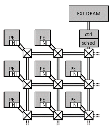
Figure 1: An example MpSoC with single external DRAM
The DRAM has undergone many innovations in the past: DDR1, DDR2, DDR3, LPDDR, and LPDDR2 (dual data-rate 1/2/3, low-power DDR) are a few technologies that have come to the market. Bus bandwidths have increased, but fetch time hasn’t changed significantly. Correspondingly, the memory controller and the memory scheduler have been undergoing several innovations. In fact, the DRAM controller is a complex piece of intellectual property with single ported controller itself in the range of 50 K gates [8]. Trying to mimic them accurately can be a time consuming task. Further, as the technology evolves, the models need to be maintained and enhanced accordingly. Finally, many of these controllers are developed in-house with proprietary technology. This makes mimicking these controllers much more difficult.
While effective modeling of the DRAM memory subsystem is essential in evaluating the NoC realistically, accurate modeling may not be practical due to the issues identified above. This article focuses on effective modeling of the controller. We identify essential characteristics that affect the DRAM efficiency, and propose an abstract modeling paradigm for them. Such models can then be plugged into the SoC environment for performance analysis. Abstracting the implementation to a higher level helps us in generalizing the problem enough to be able to apply the model as a general memory subsystem, as opposed to vendor specific memory subsystem. In the following sections, we will present the essential DRAM characteristics, and then provide the modeling framework.
2. DRAM Characteristics
Wang et al [10] provide an excellent discussion on DRAMs and their performance evaluation. A DRAM is typically organized as a set of banks, where each bank is composed of a set of rows, and each row is composed of a set of columns. This is described in Figure 2.
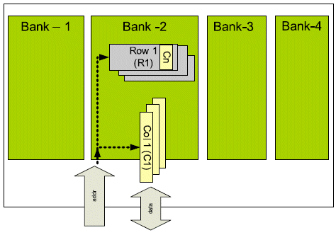
Figure 2: DRAM organization in terms of banks rows and columns

Figure 3: Format of DRAM address
It is possible to interleave operations to multiple banks of memory, thereby increase effective bandwidth. A bank is either idle, active, or changing from one to the other. At the beginning of read or write operation, a bank must first be activated based on the incoming address. This does not affect other banks because banks are independent. At the same time, the accessed row will become active and after that accesses to certain columns are possible. Hence, it takes some time to read the first data but the consecutive ones come faster.
The width of the address depends naturally on the memory size, for example a 128 MB memory requires log2(128M)=7b +20b=27 bits. The address organization is depicted in Figure 3. Although Figure 2 suggests a hierarchical organization of the addresses, the DRAM addressing is usually organized by placing the bank decode bits in between the column bits and the row bits. The “Min Bytes” box denotes the DRAM data width. DRAMs used in high performance SoC may typically have data width range from 2 to 8 bytes1. To this end, the minimum number of bits needed to represent the DRAM data width may be calculated as the log2(data width in bytes). The DRAM BL (or burstlength) denotes the minimum granularity at which DRAM accesses are done. In other words, each access to the DRAM always returns BL number of transfers for RD, and writes BL number of transfers for WR. DRAM BL, multiplied by the Min Bytes, thus returns the minimum number of bytes that are transferred per access. BL is usually constant per DDR type. For example, DDR-2 allows BL of 4 or 8, but DDR-3 imposes a BL of 8.
The column bits, which start at the top of Min Bytes and go until the start of the Bank bit, denote the number of columns bits per row. Typically, there are 1024 columns per row which means 10 column bits. Once the row is activated, multiple accesses from that row may be performed with minimum latency. On the other hand, latency for access is maximized when i) the DRAM is refreshed and ii) when the row has to be closed and a new row has to be opened. The DRAM requires periodic refreshes to keep the data active. These refreshes require the active row to be closed down, followed by the refresh operation. A request that arrives during this operation must wait for the refresh to be completed before accessing the DRAM. The other reason for increased latency is called the page miss. When a particular row is active, and a request is for a different row in the same bank, the active row must be closed and the new row must be opened. This incurs a latency penalty due to the time it takes to close the row and activate a new row.
As mentioned before, the bank bits are interspersed between the column and the row bits. A linearly increasing address will therefore hop banks before hopping rows. Hopping rows on the same bank requires the currently activated row to be closed, and a new row to be activated. Due to the electrical characteristics of the sense amplifiers inside the DRAM, this operation has a significant latency associated with it (in the range of 50-60 ns). However, the DRAM allows multiple banks to be open at the same time. Hence, hopping banks allows for better DRAM utilization than hopping rows. Figure 4 explains this phenomenon by means of an example. The left part of the figure depicts a case where multiple requests are sent to the same bank, but different rows. Therefore, before each request is serviced, the DRAM controller has to close the previous row and open a new row, thus incurring a fixed latency for the request. Hence, two requests are interspersed by a number of idle cycles. The right part of the figure depicts the case where the requests are interleaved between banks. Note that DRAMs can keep multiple banks open at the same time. This provides the controller to send a set of requests to the different banks, and thus amortize the latency. This reduces the number idle DRAM cycles, and thus improves efficiency.
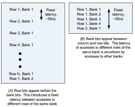
Figure 4: Advantage of bank interleaving of requests
3. DRAM Latencies
In order to do performance analysis of a NoC, the important DRAM parameters have to be identified. From the NoC perspective, the important parameters are those that have maximum impact on the arbitration schemes inside the NoC. In other words, if a different arbitration inside the NoC can significantly affect the latency due to a given parameter, the parameter is an important component of the DRAM model. The DRAM bus frequencies have recently increased from 133 MHz to 200 MHz, and then to 400 MHz and 800 MHz. However, the following parameters are mostly independent of the transfer bandwidth and DRAM’s bus frequency. Consequently, the number of required cycles increases with newer memories. Memory modeling can be correspondingly simplified by associating fixed latency for each of the parameters that impact the NoC performance. The important parameters are described below. The values corresponding to these parameters can be found in either the DDR model specification (for example, Micron DDR model [11]) or the JEDEC (Joint Electron Device Engineering Council) specification [10].
1. Access Granularity
DDR memories specify a minimum access granularity per request. A RD request must be of a certain size (computed in bytes). The parameter controlling this in the DRAM is the DRAM burstlength (BL). The DRAM burstlength denotes the number of data words written for WR accesses (or read for RD accesses) per access to the column. This phenomenon is described in Figure 5. Any access to the DRAM must be B x BL number of bytes, where B is the data width in bytes. Since DDR memories use both edges of the clock, this access takes BL/2 number of cycles. If the size of the request is less than B x BL bytes, the DRAM will still use up BL/2 cycles. For example, assume BL = 4, and B = 4. Assume that a request has a size of 8 bytes. It should take 8/ (Bx2) = 1 cycle to service all data words of this request. However, this request will be serviced in BL/2 = 2 cycles, thus introducing one idle cycle in the bus. Hence, this affects only transfers that are less than the minimum granularity
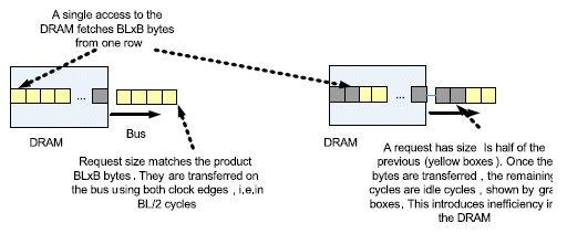
Figure 5: Impact of DRAM burst length BL being larger than 1 word. The size of the word is B bytes, depending on the DRAM.
2. DRAM Refresh
DRAM needs to refresh its rows periodically to retain data. During refresh, no operation is allowed in the DRAM. Refresh can be modeled to occur once every N nanoseconds, when N is usually around 7600. The duration of refresh is around 120 ns. This translates to roughly 130K refreshes per second which reduce the bandwidth by 120/(120+7600) = 1.5%.
3. Maximum number of open banks
Within a window of Tfaw nanoseconds, at most 4 row activation commands can be issued. Note that row activation command refers to the command that opens a row in a bank. Tfaw is typically around 40 ns.
4. Page Miss to the Same Bank:
Two accesses to the DRAM, each going to the same bank address, but different row address should be separated by Trc nanoseconds, where Trc is typically 55 ns.
5. Row Activation Latency
This is the time that must elapse between activate commands to two rows in different banks. This is denoted as Trrd and is typically around 10 ns.
6. Precharge Command Period
There is a latency associated with the time it takes to close a page. This is called “precharge command period”, and is denoted by Trp, which is around 10 ns
7. CAS Latency
A fixed latency is associated with each RD access and the time the first data is available in the output pins. This latency CL is typically around 10 ns.
8. Minimum delay between two column accesses
Two column accesses must be separated by a minimum delay called Tccd, which is typically 1 cycle for DDR1, 2 cycles for DDR2 and 4 cycles for DDR3. Note that while many other parameters are measured in nanoseconds, Tccd is measured in cycles, thus making it bus frequency dependent.
9. Write to Read Turnaround Penalty
A write request followed by a read request consists of a Twtr penalty. It is independent of the addresses of the corresponding requests. Note that JEDEC does not specify a similar command from read to write. The parameters mentioned above are largely technology independent. There is usually a small variation depending on the type of memory being used (DDR-1, 2, or 3). Exact values can be obtained from the corresponding JEDEC or memory specs [10, 11]. Note that the list of parameters mentioned above is not exhaustive. However, the parameters mentioned above are the critical ones that affect the performance of the DRAM subsystem significantly. An exhaustive list can be obtained from JEDEC specification or a DRAM model specification.
4. Examples
The following tables provide some examples of the DRAM latencies for different configurations. In the calculations Tfaw, CL and Tccd have been ignored. This is because many controllers are able to amortize the latency due to these parameters by pipelining the operation. Table 1 denotes the values assumed for the different DRAM parameters. Table 2 provides the description of a scenario for each results table. Table 3 through Table 6 provides DRAM performance values for different scenarios. In each table, the first column denotes the number of transfers before a page miss occurs. The second column denotes the latency for the set of transfers in nanoseconds. The third column denotes the average latency per transfer, which is obtained by dividing the latency by the number of transfers (value in column 1). Finally, the fourth column denotes the efficiency of the system if such a pattern was repeated. Efficiency is calculated as a fraction of the maximum bandwidth (0-100%). We assume that at the start of the request, the request pays a penalty (such as page miss penalty). The remaining transfers are then serviced at maximum efficiency. For example, in Table 3, the fifth column assumes that the first transfers pays the trc, twtr and trp penalties, and the remaining 31 transfers are serviced at maximum efficiency. The resulting length between page misses is affected by both the access patterns of the program and the DRAM scheduler/controller. In the worst case, the dependencies between memory references prevent scheduler from optimizing the DRAM accesses, and there will be many page misses.
Table 1 Parameter summary

Table 2: Description of tables

Table 3: Typical latency values (Trc, Trp, Twtr)
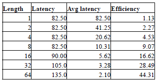
Table 4: Typical latency values (Trc, Trp)
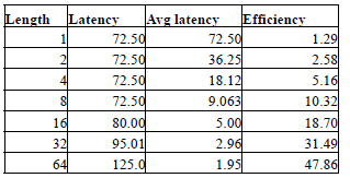
Table 5: Typical latency values (Twtr)
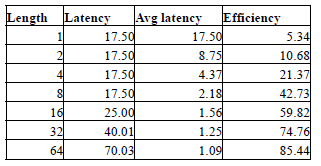
Table 6: Typical latency values, best case
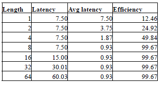
from the table above, it can be noted that even under the best case, the DRAM performance can be severely affected by short bursts. In all cases, having just 4 transfers results in half the efficiency compared to 8 transfers (which is equal to DRAM burst length). For example, efficiency is less than 50% even in the best case and less than 5% if one accounts the three latency components.
A system with a high page miss rate and direction turn around rate (Table 3) will be severely affected even if the penalty is paid only once in 64 transfers. The last column of Table 6 is the best case, which essentially denotes 100% efficiency, is usually purely theoretical and is usually never achieved. Typical DRAMs operate at efficiencies ranging from 50% to 85% depending on the nature of the applications.
5. Conclusion
System-on-Chip designs incorporating a NoC are constrained by limited memory efficiency. Therefore, performance analysis of the NoC that is agnostic to the memory requirements may result in overly optimistic results, which may not be reproducible in the real system once the DDR memories are incorporated. Performance analysis in memory agnostic environment can therefore result in surprises late in the design cycle, and possibly a requirement to re-architect the NoC due to the performance implications of the memory subsystem. This will significantly delay the time to market of the SoC.
Table 7: Summary of DRAM model parameters
| Non-ideality | Modeling parameters |
| Small accesses reserve the bus for longer time than necessary | Burst length BL is 2 words for DDR1, 4 words for DDR2, and 8 words for DDR3 |
| Refreshes prevent regular accesses | Tref: Duration 120 ns, period 7600 ns |
| Bank activation takes time | 4 banks opened per Tfaw, Tfaw = 40 ns Trrd = 10 ns |
| Row activation takes time | Trc = 55ns |
| Column access takes time | CL = 10 ns delay before first read operation Tccd = 1, 2 or 4 cycles for DDR-1,2,3 respectively, for the consecutive column access |
| Write must complete before read | Twtr = 7.5 ns |
| Closing a page takes time | Trp = 10 ns |
On the other hand, modeling a DRAM memory subsystem accurately may not be practical, given the effort involved, the tendency of going for proprietary controllers, and the constant evolution of the controllers from one generation to another. In this paper, we have identified a list of parameters that are the major contributors to DRAM inefficiency, see Table 7 for summary. With these parameters, a highly abstracted model of the DRAM controller can be modeled reasonably quickly. This model can then be plugged into the SoC performance model, instead of dumb slaves. Analysis with this system will provide the SoC designer with realistic performance numbers. The designer can then tune the NoC accordingly early in the design cycle and thus achieve faster design closure.
6. Acknowledgements
We would like to acknowledge the important suggestions provided by Dr. Zhonghai Lu, Royal Institute of Technology (KTH), Stockholm, and Dr. Drew Wingard, CTO, Sonics Inc.
7. References
[1] T. Bjerregaard and S. Mahadevan, “A survey of research and practices of network-on-chip,” ACM Computing Suveys, vol. 38, no 1, p. article No, 1, 2006.
[2] C. Grecu, A. Ivanov, A. Jantsch, P.P. Pande, E. Salminen, Umit Ogras, Radu Marculescu, "Towards Open Network-on-Chip Benchmarks", First International Symposium on Networks-on-Chip (NOCS'07), Princeton, New Jersey, USA, May 7-9, 2007, pp. 205-205, IEEE.
[3] E.Salminen, "On Design and Comparison of On-Chip Networks", PhD Thesis, Tampere University of Technology, Publication 872, 2010, 230 pages.
[4] K. Srinivasan and E. Salminen, “A Methodology for Performance Analysis of Network-on-Chip Architectures for Video SoC”, OCP-IP, [online], April 1, 2009, 10 pages.
[ 5] E. Salminen, A. Kulmala, T.D. Hämäläinen, "On Network-on-chip comparison", Euromicro conf. on Digital System Design, Lübeck, Germany, August 27-31, 2007, pp. 503-510.
[6] I. Walter, I. Cidon, R. Ginosar, and A. Kolodny, "Access regulation to hot-modules in wormhole NoCs," in NOCS, May 2007, pp. 137-148.
[7] W. Wolf, A.A. Jerraya, G. Martin, "Multiprocessor System-on-Chip (MPSoC) Technology," Computer-Aided Design of Integrated Circuits and Systems, IEEE Transactions on , vol.27, no.10, pp.1701-1713, Oct. 2008,
[8] DDR controller, Comit Systems
[9] D.T. Wang, “Modern DRAM Memory Subsystems: Performance Analysis and High Performance, Power Constrained DRAM Scheduling Algorithm”, Doctor of Philosophy Thesis, Department of Electrical and Computer Engineering, University of Maryland, College Park, 2005.
[10] Joint Electron Device Engineering Council, JEDEC Specification, www.jedec.com
[11] Micron Technology Inc., Micron DDR2 specification
1 64 bit DRAMs can be composed of multiple 16 bit DRAM parts