Manuel Mota, Synopsys
Introduction
Design teams tackling mixed-signal system-on-chip (SoC) designs face the problem of how to get the most out of advanced process technologies when it comes to implementing their analog IP. They need to take a different approach to mixed-signal design and utilize analog architectures that better suit the latest digital process technologies.
Applications that typically depend on mixed-signal SoCs include mobile communications, wireless applications and multimedia devices, such as set-top boxes and digital TVs. They need to take analog signals from radio transmitters, wireline transceivers and sensors. One of the key tasks for mixed-signal SoCs is to convert the incoming analog signal to a digital signal for processing on the chip using an accurate analog-to-digital converter, or ADC.
According to Moore’s Law, SoC density is expected to increase by 1.5X-2X in every new process generation, and power consumption must reduce by the same factor.. However, analog components cannot immediately take advantage of feature size reductions. In fact, dynamic range and accuracy requirements limit area and power consumption irrespective of process improvements. To achieve scaling factors similar to digital circuits, analog circuits must exploit the higher speed and processing power made available by Moore’s Law scaling. For example, more compact analog blocks can perform the same functions of more complex ones by relying on digital compensation, calibration, and higher processing speed, leading to the concept of digitally enabled analog circuits.
This paper elaborates on how ADCs can work with Moore's Law to move with the power and area scaling trends that are common for digital circuits. It will:
- Compare the main ADC architectures and conclude that the Successive-Approximation Register (SAR) based ADC is very well positioned as the architecture of choice for medium- and high-speed ADCs in modern SoCs, especially in 28-nm processes and beyond.
- Describe implementations of the SAR ADC architecture that reduce power consumption and area usage dramatically, enabling SoC designers to successfully integrate these analog components in their next SoCs.
ADC Architectures
Today, design teams can choose from a number of different ADC architectures, like Pipeline, (Successive-Approximation Register) SAR, Sigma-Delta, and Flash. Each architecture has different characteristics – some are better at supporting higher resolution accuracy, while others offer better support for high sample rates.
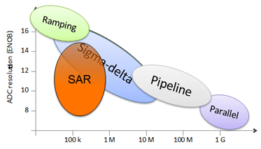
Traditionally, they are distributed as shown in Figure 1.

Figure 1: Traditional areas of application of ADC architectures
Each ADC architecture brings its own merits:
- Flash, or Parallel, architectures perform the data conversion in a single step, making them very fast. However they can be power hungry and their analog circuit count increases exponentially with the number of bits, so its usage is typically limited to low-resolution applications.
- Ramping architectures perform the conversion by measuring the amount of time it takes for a slow reference ramp to cross the input signal level. These converters can achieve very high resolution but are limited to very slow applications.
- Sigma-delta architectures use high oversampling rates and noise shaping techniques to create a high-speed bit stream whose density accurately represents the input signal. The digital representation of the input signal results from the accumulation of a long period of the bit-stream, yielding a relatively slow effective conversion rate. This characteristic makes them useful especially for high-resolution, low- to moderate-speed applications.
- Pipeline architectures make use of cascaded conversion stages, each performing a very fast low resolution conversion, followed by the calculation of the residue that is provided to the next stage for further processing. The fact that the conversion is achieved with multiple, similar, successive steps yields a modular architecture. This architecture can deliver medium resolution (10- to 12-bit) and high speed (up to 100’s of MSPS). However, latency can be high due to the sequential nature of the conversion.
- The SAR architecture digitizes the input signal step-by-step by running a successive approximation algorithm and determining each bit one by one until the complete conversion is finalized. This architecture reuses the same hardware for each step; therefore, it requires a high clock rate to complete the conversion before the next sampling instant. For example, a 11x clock rate may be used for a 10-bit ADC. Consequently, this architecture has traditionally been limited to low-speed, medium- to high-resolution applications.
Table 1 summarizes the key tradeoffs of the ADC implementations shown in Figure 1.
Table 1: Trade-offs of ADC architectures
| Architecture | Latency | Speed | Resolution | Area and power consumption |
| Flash | Low | Very high | Low | High |
| Ramping | High | Very slow | High | Low |
| Sigma-delta | High | Slow-medium | High | Medium |
| Pipeline | Low-medium | High | Medium | Medium |
| SAR | Low | High | Medium-high | Low |
SAR ADC architecture for high speed and low power at 28-nm and below
Given the high speed and processing power achieved with modern process nodes, at 28-nm and below, the SAR ADC is becoming very competitive and thus the subject of deeper scrutiny. In fact, The architecture is very efficient, even where pipeline or parallel ADCs had been the norm [1].
One interesting aspect of the SAR architecture is its inherent simplicity. In contrast to other ADC architectures, the SAR ADC implementation does not rely on having multiple stages with large, power-hungry gain amplifiers. The analog element of the design is a single-stage comparator, which is inherently compact and low power. Another benefit is that unlike many analog structures, the SAR ADC is not overly sensitive to the analog characteristics of the silicon process for correct operation.
SAR architecture basics
Figure 2 shows the basic block diagram of a SAR ADC including a sample-and-hold (S&H), a comparator (Comp), a DAC and a logic block (SAR). The input signal (Vin) is stored on the sample-and-hold and is successively compared to the output of the DAC, whose input codes are set by a logic block depending on the result of the previous comparisons.

Figure 2: Basic block diagram of a SAR ADC
The logic block controls the search for the code that represents the input signal level. this algorithm is called Successive-Approximations and starts by comparing the stored input signal with the mid-range of the ADC, by asserting the Most Significant Bit (MSB). The output of the comparator will tell if the input signal is on the upper or lower half of the range and set the MSB accordingly. Next, the second MSB is asserted allowing to further test on which half of the already resolved range the input signal is; this process continues until the Least Significant Bit (LSB) is resolved. The process takes N steps for an N-bit ADC.
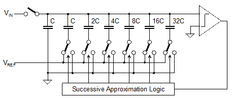
The beauty of this architecture is that no power hungry precision amplifier is required, as it employs only blocks that can be designed with zero static power consumption. Moreover, the sample-and-hold can be merged with the DAC by the use of switched capacitors, further reducing the area and eliminating interfaces. Figure 3 shows a simplified schematic of a SAR ADC for 6-bit resolution. The input signal (VIN), is initially sampled on the top-plate of the capacitor array. Next, with the top-plate now floating and storing the input signal, the individual bit weights are subtracted by switching the bottom plates of the capacitors from the reference voltage (VREF) to ground, starting with the MSB. When switching the capacitor 32C to ground by setting bit 6 to “0”, a step of VREF/2 is subtracted from the array top plate. If the input signal value is below VREF/2 the comparator produces a logic “0” at the output, fixing the bit 6 at “0”. Otherwise, if the input signal value is above VREF/2 the comparator produces a logic “1” at the output, returning the bit 6 to “1”. The process continues with capacitor 16C (that subtracts a step of VREF/4 from the array top plate) to determine bit 5, and so on, until bit 1 is reached and the conversion is complete.

Figure 3: Simplified schematic of a 6-bit SAR ADC
Evolving the SAR architecture for high speed and low power
The traditional topology described above is simple; however, it is inherently slow and makes use of large capacitor arrays for moderate and high resolutions, which impact both area and power dissipation. On the other hand, this topology can be improved with a multitude of techniques that fully exploit the architecture potential for low power and increase the conversion speed.
Reducing clock speed requirements
The need of a high frequency clock is removed by controlling SAR and DAC blocks (Figure 2) with an internal clock that is asserted every time the comparator completes a decision. This is possible since the comparator can produce a logic signal when it completes a comparison: typically, before comparison its two differential outputs are both reset at VDD (or ground depending on the implementation), and after the comparison they become complementary. Therefore, an NAND gate produces a logic “1” when one of the outputs reaches “0,” indicating a decision was reached (an OR gate is used for reset to ground). This signal, together with a delay block, can then be used to sequence the bit decisions in succession until the conversion is complete. This way, the SAR ADC only requires a clock signal having a frequency equal to the intended sampling rate.
Reducing capacitor array
The capacitor array is binary-weighted, which means its size increases exponentially with the ADC resolution, doubling for every additional bit. For a 12-bit ADC, the capacitor array will grow 4096X over the minimum capacitance. A large capacitance leads not only to large area but also to large consumption on charging and discharging the capacitors during the conversion process. The solution to reduce the capacitance is to break the array in two by having a floating secondary array processing the lower order bits. For example, the same 12-bit ADC would have two 6-bit arrays, one to process the 6 higher order bits and another one interconnected to the first by a small scaling capacitor, Cbridge, to process the 6 lower order bits, requiring in total capacitance of only 128X the minimum capacitance.
In any case, the total capacitance of the array cannot be too small because of matching and thermal noise requirements. The matching is a function of total capacitance and, roughly speaking, errors below C/2 must be achieved on each capacitor to avoid missing codes. This will determine a minimum size for the unit capacitor C. Thermal noise also sets a minimum size for the capacitor array through kT/C, but normally the comparator noise dominates when the capacitor size already satisfies the matching requirements.
Calibrating the capacitor array
Calibration may be employed to measure capacitor matching errors, thus reducing the total capacitance to the value dictated by the noise constraint. The measurement of the matching errors can be done by observing that the nominal value of each capacitor is equal to the sum of the remaining lower order capacitors in the array. This comes naturally from the binary weighted nature of the capacitor array with an additional unit capacitor included: 32C=16C+8C+4C+2C+C+C. The process is the following: First, capacitor 32C is charged to VREF and the remaining to ground with the top plate connected to ground. Then the top plate is opened and the connections of the capacitors are interchanged. If 32C has the ideal nominal value, the voltage at the top plate remains at zero. But if there is an error, the top plate voltage will deviate showing the error and making it possible to apply a calibration method. The higher density available in advanced technologies favors the use of digital calibration techniques.
Using the capacitor array effectively
Top-plate sampling as shown in Figure 3 causes non-linearity due to the charge-injection when the sampling switch is opened. Therefore, bottom-plate sampling is typically used: it requires additional switches on the bottom-plate of the capacitors that connect to the input signal during sampling, while the top-plate switch connects to ground. Charge injection in the top-plate can now be made signal independent, thus just causing an offset which is easily corrected with calibration.
The capacitor array may consume a significant amount of power with the charging and discharging of the capacitors between VREF and ground. For example, Figure 3 shows that to determine each bit, the respective capacitor is switched to ground, but later, according to the comparator decision, it may be necessary to connect it back to VREF – this is a source of inefficiency. Alternative switching schemes can be used to save charging energy. For example, after sampling, the bottom plates can be set to VREF/2 instead of VREF, and the MSB decision can then be taken immediately. This allows saving one capacitor on the array (the 32C in Figure 3), and prevents capacitors from switching back and forth between VREF and ground during the conversion.
Improving settling time
The main limitation to speed is the time required for the accurate settling of the capacitor array in each of the bit decisions. The voltage on the top-plate needs to settle to within half the LSB weight to avoid decision errors. That is 0.01% for 12-bit conversion, requiring over nine time constants. However, in a N-bit ADC, only once during the N bit decisions is the input voltage to the comparator so small. And only the initial bit decisions need a longer time for settling because the voltage steps are progressively smaller along the conversion. Therefore, by including redundancy in the conversion algorithm, it is possible to correct for initial errors, thus allowing the bit decisions to run faster. Redundancy can be designed in by duplicating a capacitor in the middle of the array and using it to re-center the decision range even if a previous error causes the conversion to diverge.
Parallelizing for high speed
Further speed improvement is possible by time-interleaving multiple SAR ADCs. This is a common technique also used with other ADC architectures, and allows achieving high sampling rate by using several lower speed converters. Interleaving four ADCs improves speed by 4X. Naturally, any offset, gain and sampling time mismatches between the interleaved ADCs will cause pattern noise and spurs in the digitized output signal and need to be corrected by calibration.
Synopsys 28-nm SAR ADC IP
Synopsys' new generation of high-speed ADCs for 28-nm processes has migrated from the pipeline architecture to the SAR architecture, and was specifically engineered to take advantage of the high-speed of the process to minimize area and power consumption. Moreover, this architecture is likely to reap benefits similar to those observed in digital circuits when applied to even smaller process nodes: higher operating speeds with lower power and area.
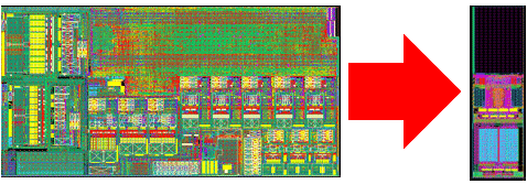
The baseline ADC resolution is 12-bit at a conversion rate of 80 MSPS. By implementing the techniques described above, an impressive 3X lower power dissipation was achieved compared to the previous generation Synopsys ADC, which had similar specifications and was based on the pipeline architecture. The SAR architecture offers a very compact structure with only a capacitor array, a comparator and a logic block, resulting in an area reduction of up to 6X (see Figure 4).

Figure 4: Layout comparison of a 12-bit pipeline ADC (left) to a 12-bit SAR ADC (right) with similar performance requirements for an LTE application (single channel example)
By interleaving two or four data converters, the conversion rate achieves 160 MSPS or 320 MSPS (Figure 5).
This ADC parallelization can be further extended to achieve sampling rates beyond 1 GSPS.

Figure 5: Modular design of SAR ADC
Achieving these large power and area reductions require a number of design techniques, some of which are made possible by the speed of the 28-nm processes:
- Internal building blocks are dynamic, resulting in a perfect scaling of power consumption with sampling frequency.
- The capacitor array is digitally calibrated to allow sizing by the noise constraint only, and not matching. The calibration is run at start-up and does not need to be updated after supply or temperature variations because only stable and drift-free capacitor ratios need to be corrected. In the interleaved construction, the calibration corrects also for offset and gain mismatches.
- Operation is asynchronous, requiring only a clock rising edge to start the conversion. The internal processing of the sampled signal and the bit decisions are sequenced by the comparator ready signal and timing circuits.
- The operation is mostly insensitive the clock duty cycle, and the ADC latency is only 2 clock cycles.
This approach is highly beneficial for design teams working on advanced devices that depend on having high-performance, low-power analog interfaces. This includes mobile communications applications including smartphones and tablets, wireless connectivity, digital TV and satellites, and many other multimedia interfaces.
