Synthesizable Verification IP
by David Murray, Duolog Technologies
Dublin, Ireland
Abstract:
Today's deep sub-micron process technology allows the creation of an incredible range of System on a Chip (SoC) based electronic products. These products, however, are sources of methodology and capability nightmares as product design teams strain to achieve the design mantra of "RIGHT FIRST TIME". This is happening across all aspects of electronic design but one common problem is common with them all – Verification. The system level verification process is the SoC ‘Right First Time' quagmire.
Various verification methodologies have evolved throughout the years that have eased the stress on this most complex part of the product design process. Block-level verification methodologies have matured to the point where they are more predictable, controllable and measurable. System-level verification methodologies, however, are strained by highly efficient SoC design capability and where a SoC can be designed in months, the system-level verification is still the high-risk, high-resource and high-stress area of the overall product design process. Today's system verification requirements are simply to get the system verification done more quickly, more safely and more smoothly. This is the requirement today but we need tomorrow's methodologies and tools to achieve it.
This paper presents an approach and case study in tackling the system-level verification problem head on. Leveraging the latest system level verification tools of co-simulation and emulation we utilise a modular synthesizable testbench that maximises the advantages and minimises the disadvantages of these methodologies. This encompasses real SoC verification IP that provides us with a reusable and innovative solution to SoC verification stress.
Synthesizable Verification IP
SoC Validation is a big problem. Design Teams have access to fast maturing SoC design methodologies giving a certain amount of ‘design-ease'. Not only can SoCs be architected relatively quickly, but by using IP Blocks, SoC architects can factor in ‘Just in Case' type scenarios – "Let's put in a USB interface just in case". The system soon becomes a spreadsheet of application configurations. In some ways the traditional pin-bound ASIC starts to look like a programmable-logic device as there can be a multitude of system-level configuration options that require validation.
Validating a system such as this becomes a very complicated task. Sub-Blocks may be 100% verified but we need to ensure that they are integrated correctly. Simple connectivity tests can be followed by sub-block integration tests to ensure that the block is connected and it alive. If there are embedded processors in the SoC we need to ensure that the system memory map is validated or we may require that an embedded operating system is validated. Once all sub-block are integrated and embedded processors are functioning correctly, we need to stress the whole system to ensure that the interconnect and system busses are performing correctly. Running actual applications on the system gives a good confidence factor and thus this should be included in the overall validation.
From integration to application level requires several orders of magnitude more processing power but with a typical system described above, combining all these levels of system validation is the only way to guarantee that your system works RIGHT FIRST TIME!
Figure 1 summarises these system validation levels.
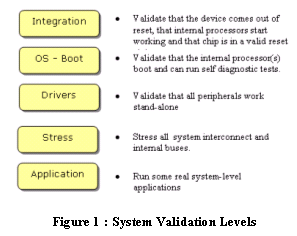
This shows us the what require for a Right-First-Time SoC validation. The problem is – How?
Clearly block-level verification methodologies and tools will not work to deliver these requirements. Standard RTL simulators are not capable of going much beyond the integration phase of the validation. Two methodologies, however, have matured to tackle these requirements. These are Co-Simulation and Hardware Emulation. While they dramatically boost the system validation process, they also have their own drawbacks.
Co-Simulation typically provides a means to run, and more importantly debug, system software on an embedded processor core. This allows software integration to take place before the chip design is concluded. The main benefits of this methodology are:
• Co-simulation allows software integration to be achieved in a fully observable environment• any real integration problems can be fixed in the hardware design
• Co-simulation is significantly faster than RTL simulation and thus can be used further into the integration validation than standard RTL.
Hardware Emulation is the means of mapping the design onto hardware. This may be programmable logic based or processor based and may be a dedicated emulation system or a simple FPGA prototyping system.
The main benefits of this methodology are:
• Speed-Speed-Speed : Emulation systems cuts simulation time by several orders of magnitude (e.g. 70,000x)• Emulation is typically derived from a pure RTL description and is a very close model of the system. FPGA based emulation can give a positive indicator of the synthesis process.
The following diagram shows the capability of different ‘simulation' methodologies with respect to our system validation levels.
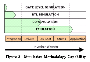
Co-simulation and Emulation also have their disadvantages. Although co-simulation can be quicker than standard simulation, it can be slow in terms of running higher-level software e.g. an operating system boot, a device driver validation or an application. Also, co-simulation is typically an optimised model of the processor with its system components and is therefore an estimation of the functionality, typically a good estimation but nonetheless an estimation.
Emulation for all its speed suffers from several drawbacks. Mapping from your design to an emulator can be fraught with difficulties and initial emulator integration can be a difficult phase to progress. Compared to the productivity gained in co-simulation and despite improvements in recent years, debugging on an emulator is still an arduous task. Also, creating tests to run on the emulator can be difficult and if real speed is required a fully synthesisable testbench is needed.
In some ways these two technologies are complementary, where one fails the other excels and vice versa. It's a battle of observability and speed. If we could bring these two technologies closer then we would benefit in many ways. Imagine if any test that was created in a co-simulation environment could be used immediately to validate your emulation mapping. Imagine creating and debugging a test case in a co-simulation environment and then running it at full speed on an emulator.
If we can combine these technologies in a reusable manner then we are creating true Verification IP and we increase our verification potential by an order of magnitude.
Our verification solution consists of a reusable synthesizable testbench that is used across all different methodologies and tools to facilitate a ‘write once – run anywhere' methodology.
A synthesizable testbench produces synthesizable test cases that can be used on any platform including :
• Co-simulation• Standard RTL Simulation
• Gate Level Simulation
• Emulation Simulation
The main benefits of a modular synthesizable testbench are :
• Co-simulation can be used to debug test cases. The full observability allows hardware validation and software integration to work at maximum productivity. Once the co-simulation is delivering self-contained test-cases, these can be used as a confident entry point into hardware emulation.
• The emulation system can be initially validated using tests from the co-simulation process. This cuts out the primary drawback of emulation which is the debugging process to get tests working. Once the emulation database is validated the test cases can be expanded. Emulation is therefore used primarily for finding bugs and not debugging test cases
• The testbench does not have to be recompiled for different test cases and so has stability across all platforms
• The testbench is a HDL only testbench and can be built/extended by anyone familiar with the HDL. These test cases themselves are synthesizable and thus targeting different simulation/emulation/prototyping systems is feasible. Also, there are no extra tools required or extra languages needed for modelling the testbench.
• A Synthesizable testbench allows for the fastest emulation speeds.
Of course synthesizable testbenches have their own problems :
• A typical synthesizable testbench is hard to control . How are test cases written?
Our solution tackles these problems to create the ultimate synthesizable testbench.
The Modular Synthesizable Testbench
For SoC validation we use a single testbench architected out of Synthesizable Testbench Modules (STMs) as shown in Figure 3.
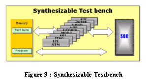
All testsuites are memory based providing concurrent control and data to the STMs.
STMs give the testbench a modular architecture and indeed the STMs are architected to resolve specific problems inherent in a synthesizable testbench . The whole methodology centres around a synthesizable component called the C3 (Concurrent Controller Core).
Testbenches typically are discarded because their inherent structure is not reusable. With the C3, however, the level of abstraction is raised and this promotes reusability.
The C3 is essentially core Verification IP from which other higher level blocks are easily constructed.
Synthesizable Testbench Module (STM)
The following diagram shows the structure of an STM:
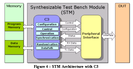
The STM is a reusable testbench component that is 100% synthesizable and can be considered the verification equivalent of a standard design IP Block e.g. UART, I2C, UTOPIA, LCD, PLCP etc.
These STMs are the main components of a plug and play testbench which can be quickly constructed from a component library to provide a concurrent, realistic platform for SoC validation or intensive block level validation
Each STM contains a C3 that provides a wide range of programmable verification functions. The STM also contains a Peripheral interface (PI), a custom block which provides the specific STM functionality e.g. UART. Using this methodology each STM can be independently programmed , a critical feature of a SoC validation environment. Also, the advantage of this generic approach means that the programming of all STMs is similar.
Synthesizable testbenches can also have non-C3-based STMs such as Flash Memories or SDRAM interfaces.
Concurrent Controller Core (C3)
The C3 is an advanced programmable controller designed specifically for complex verification environments. It provides independent, concurrent control of its host STM within a validation environment. The C3 has a generic instruction set for data path management, Master/Slave mode configuration and synchronization. This instruction set is typically extended to cover STM Specific configuration and control.
The following are the primary features of the C3:
• Configure any STM parameter via extendable control/config interface• Send control pulses to the STM
• Send/receive specific lengths of data from/to memory. Data can 8/16/32 bit
• Send/receive specific lengths of pseudo-random data. This allows scoreboarding or self checking data transactions
• 16 configuration mode possibilities (Master/Slave/Freerun)
• Time-based or event-based synchronization
• Configuration of 8/16/24/32 bit data interfaces
• Generic status reporting
• Simple connectivity to Peripheral Interface.
Software tools are used to extend the functionality of the C3 so that new configuration or control mechanisms are seamless to the operator.
Programming the C3
The C3 is controlled through a simple scripting language which is automatically extended as more commands are added for specific STMs. At simulation start these scripts are translated into opcodes and loaded into specific memory locations. An example of a script is as follows:
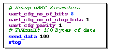
The ‘uart_cfg' commands are specific to a UART STM and the send_data and stop commands are generic C3 commands i.e. the send_data command will work on any STM that has transmit capability.
Synthesizing the C3
The C3 is fully synthesizable and, in standard configurations, it is about 3.5K Gates. It can be further optimised by reducing the feature set e.g. removing redundant data paths and data widths.
A Sample STM
The following diagram shows a high-level diagram of how the C3 can be used as part of a Camera interface emulator.
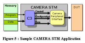
In order to test and integrate the camera interface the following is required :
• Camera Interface Transmission to DUT in accordance with specific protocol Configurable Image Size, Image mode
The C3 is used as data transmitter using the C3's generic send_data command. The size of the data stream is selected with the C3's generic data_size configuration command.
The Camera PI interfaces to the C3 via a simple state machine. This PI acts as a simple bridge between memory and the Camera Protocol transmitting memory data containing headers + image data.
Alternatively, the C3 and PI can be extended to have image size and mode etc. as parameters. Once transmission is indicated from the C3, the PI generates header information based on the input parameters. It takes pure Image data from memory and sends this on the camera interface.
The Camera Peripheral interface is less than 500 gates in the first instance and less than 1K gates in the second so the design of this block is trivial.
Note: These STMs can be re-used in any C3-based testbench , without any change.
System Level Stress Testing
STMs can be programmed to send or receive :
• Application data from memory.
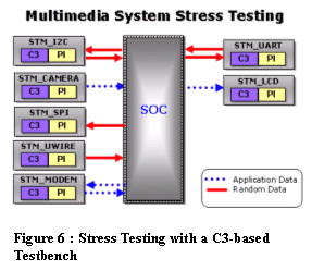
A stress test scenario can be setup within a co-simulation environment and later run on an emulation environment. A typical stress test, as illustrated in Figure 6 includes setting up self-checking point to point data transactions that run continuously in the background. This is implemented by generating pseudo-random data from source C3s and checking the data stream with target C3s. They require the same seed and some software routines in the core processor to transfer data from one peripheral to the other. e.g. from UWIRE to SPI. This type of transaction can be seen as continuous self-checking background noise.
While these self-checking transactions are running in the background, real application test cases can be implemented e.g. taking raw data from the CAMERA, processing it and transmitting it to the LCD. This provides an efficient way to stress system interconnect while directed system behaviour is validated.
Case Study : Multimedia Platform Validation : Use of C3 within an emulation environment.
Device : Dual Processor based SoC
Testbench : 15 STMS
Technologies : Co-simulation + HW Emulation
Highlights :
• The C3-based architecture was validated at an early stage on the HW Emulator
• C3-based testbench development was highly productive
• C3-based technology allowed all SW Development a single view of the testbench
• TB validated independently of design on RTL and emulation platform
• Emulation integration tests developed in co-simulation environment with automatic porting
• Fully automated porting of test cases.
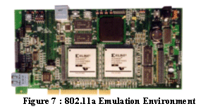
Case Study : 802.11a Platform Validation
Device : Internal IP core
Testbench : 4 STMs
Technologies : Matlab modelling, RTL simulation + FPGA prototyping.
Highlights :
• 802.11a Baseband Validation. C3-based STMs allow configuration of PLCP/RF interfaces.• PLCP, RF, control and monitor STMs.
• Synthesizable channel model for multipath delay + parameterizable noise sources.
• C3-Based control + monitoring STMS to allow programmable monitoring of critical internal signals
• Matlab-Emulation-Matlab flow
Applications
The C3-based testbench methodology has a wide range of applications. The C3's configurable and programmable nature means that it is highly adaptable. The following are a list of application areas for the C3
• A Data Engine. The C3 acts as a controllable data engine and is be used to transmit or receive directed or random traffic. This could be data from any framing protocol, SDH, ATM, HDLC, DPLD or from standard peripherals e.g. I2C, SPI, uWire, I2S, UART.
• A Control Processor. The C3 can be used to control the testbench and can be typically used to reset the SoC and enable other processes. Some other typical functions are to control pin demultiplexing of a pin-multiplexed SoC or to control interface loopback.
• A Test Processor. The C3 can be used to emulate JTAG or Test control.
Because the C3-based methodology is derived from VHDL it can be used in any platform. It can be simulated, co-simulated, accelerated emulated or prototyped.
The Future.
The C3-based synthesizable testbench is enabling a ‘virtual prototyping' type methodology. This means that if we have access to programmable logic, be it a custom emulation board with FPGAs or an off-the-shelf emulation system then we can compile our complete design + testbench + test cases onto this and run real system tests. Alternatively, we can combine this methodology to boost our current prototyping environment by connecting the SoC to devices which do not exist on the prototyping board. Either way the modular synthesizable testbench has very far reaching and very positive implications for SoC Verification.
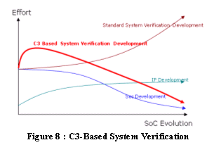
Figure 8 shows that any investment in the reusable testbench will ensure that future verification projects are fractions of the development time instead of the primary development effort.
Conclusion
The C3-based Synthesizable Testbench methodology has many benefits. It provides a completely reusable testbench architecture which can be reused both across different methodologies and across different projects.
We have been able to write test suites within a co-simulation environment that have ported automatically to a target emulator. The validation team using the C3-based testbench have developed their own modules in dramatically reduced schedules. Software integration teams have a simple and generic view on how to program the testbench. As the testbench is modular, any STM developed can be reused instantly within another testbench environment.
The approach is standardised, the benefits - huge, the learning curves - easy and the reusability - ensured, leading to reduced schedules for SoC validation and overall verification stress.
Related Articles
- Supporting hardware assisted verification with synthesizable assertions
- Synthesizable verification IP speeds design cycle
- EAVS - Electra IC Advanced Verification Suite for RISC-V Cores
- Hardware-Assisted Verification: The Real Story Behind Capacity
- How to Save Time and Improve Communication Between Semiconductor Design and Verification Engineers
New Articles
- Optimizing 16-Bit Unsigned Multipliers with Reversible Logic Gates for an Enhanced Performance
- How NoC architecture solves MCU design challenges
- Automating Hardware-Software Consistency in Complex SoCs
- Beyond Limits: Unleashing the 10.7 Gbps LPDDR5X Subsystem
- How to Design Secure SoCs: Essential Security Features for Digital Designers
Most Popular
- Automating Hardware-Software Consistency in Complex SoCs
- System Verilog Assertions Simplified
- Enhancing VLSI Design Efficiency: Tackling Congestion and Shorts with Practical Approaches and PnR Tool (ICC2)
- System Verilog Macro: A Powerful Feature for Design Verification Projects
- Optimizing 16-Bit Unsigned Multipliers with Reversible Logic Gates for an Enhanced Performance
|
|
E-mail This Article |
|
Printer-Friendly Page |


