A Flexible Business Model from Hyperstone
by Axel Mehnert, Director Marketing, Hyperstone AG, Konstanz, Germany
Dr. Matthias Steck, VP Sales & Marketing, Hyperstone AG, Konstanz, Germany
Peter Duchemin, CEO, Smart Network Devices, Juelich, Germany
Peter Eckelmann, Product Line Manager, AK-Elektronik, Hilgertshausen, Germany
The "System on Chip" (SoC) concept has, in the last few years, been bounced from ‘pure hype' to ‘already dead'. This stance may be explained by many suppliers setting up their business models to support either the "standard processor" model or to provide intellectual property (IP) and/or services for the SoC development model. However, one company – Hyperstone – serves both models in order to maximize customer benefit and support those customers who need standard products initially, and IP and services later, as their products mature and improve.

Standard Processor vs. SoC Based Application Design
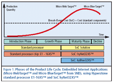
The number of units produced over time can change and usually depends upon the product maturity level as described by the Product Life Cycle Theory (see Figure 1). At the same time, the decision to base an application's design on standard processor chips or on a specifically customized "System on Chip" (SoC) solution, will depend upon any planned production quantities. The advantages and disadvantages of each approach can be seen in Table 1 (page 9). From the market introduction through to the growth phase, it may make sense to base products on standard processors, as any expected volumes should be relatively low. In addition to that, numerous factors such as risk (in terms of market success), development costs, and the market entry time, do not necessarily support an investment in an SoC design. However, as the product matures, production volumes may increase and an SoC development may become advantageous, reducing unit costs as soon as the break-even point is achieved. Additionally, such factors as increased power efficiency and decreased footprint, help improve product quality and competitiveness. Finally, considerations about the verification of demand, creation of barriers to competitive market entry, and preparation for potential price wars may convince the management that a transition towards an SoC design is a valuable (and viable!) investment. While developing and phasing in the SoC, it is important to maintain sufficient production quantities at sustainable quality levels. During this phase, many organizations realize that their core competence is not in SoC design – suppliers and partners that have provided standard components do not offer the required products and services, and software may need to be adapted to new components – leading organizations to seek out new partners. In order to minimize potential pitfalls, the availability of a compatible processor IP or adequate support from the supplier during the SoC development is essential.
The Flexible Business Model
Hyperstone customers do not have to change suppliers as products evolve; various standard processor chips are available to start the product design and to produce volumes for market introduction. Customers can later integrate Hyperstone's synthesizable, single-core RISC/DSP macro cell into their own SoC design, as well as using Hyperstone's know-how and resources to support their own design activities. Together with its network of partners, Hyperstone can offer turnkey solutions and fulfill any outsourcing needs. Customers have the option to either license the IP, or purchase the finished SoC from Hyperstone (who are operating as general contractor). Hyperstone-based applications typically require a reasonable RISC/DSP performance with minimal production costs and minimal power consumption. Without additional hardware, it is possible to include functionalities such as real-time SSL encoding, image compression (JPEG, MPEG) for embedded web cams, soft modems for direct Internet access and many other signal processing protocols needed e.g. for communication via Bluetooth™.

The World's Smallest And Most Energy Efficient 32-Bit RISC/DSP Processor
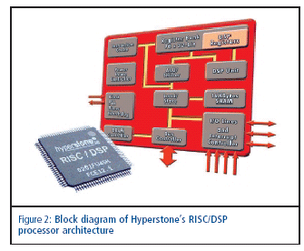
The Hyperstone RISC/DSP processor unifies a 32-bit RISC CPU with a DSP unit in a single core (Figure 2). The instruction set is variable with lengths of 16, 32 or 48 bits and while instructions for frequently used operations have been coded into 16-bit commands, rarely-used functions and long commands have been encoded in 32 or 48 bits. The architecture has a single instruction stream for logic and DSP instruction, and all units are shared between logic and DSP instructions, resulting in a low total gate count of 35,000. The CPU and DSP unit are connected via a set of 96 registers of 32 bits each. The DSP unit is based on a 16x16-bit multiplier and a 64-bit adder. This key 16-bit multiply accumulate is executed in one clock cycle (pipelined) and 32- and 64-bit operations are implemented as well.
Parallel Processing Improves Real Time Performance
The pipelined processing of the RISC and DSP units allows execution of most instructions in one clock cycle and up to four operations can be executed per clock cycle. At processor clock frequencies of up to 220 MHz, this results in up to 880 MOPS (million operations per second). A good example of the efficiency of this design is the inner loop of a Fast Fourier Transformation (FFT) that simultaneously loads new data while multiplying. By doing so, the FFT optimally utilizes the parallel processing design capabilities and achieves a respectable performance of 0.25 ms for a 1k complex FFT with 16-bit data. This performance level can only be matched by dedicated DSP's, and outperforms all other microcontrollers without an integrated DSP unit.

Direct Addressing of External DRAM
Hyperstone's RISC/DSP processor includes 16 KBytes of static RAM. The programmable on-chip memory controller controls and optimizes access to five independent address spaces, each with individual bus width and bus timing. It directly controls fast page mode RAM's, EDO RAM's, and synchronous DRAM (SDRAM) without the need for any additional external logic. The refresh is managed internally and this allows the design of extremely compact systems to the point where only processor and memory is required.
Energy Saving Features
The RISC/DSP processor integrates a 32-bit watchdog timer, an interrupt controller for internal interrupts, and seven priority-controlled external interrupts. An on-chip phaselocked loop (PLL) controls the internal processor clock and can be determined by using almost any type of external clock generator. The frequency can be controlled and changed by software during program run time. The timer settings or dividers can be altered in order to minimize the energy consumption and to adjust the provided performance as needed. Additionally, the Hyperstone processor provides several energy saving modes, reducing power down to less than 100µA.
Embedded Internet using the Hyperstone Standard Processor
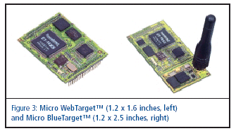
Smart Network Devices (SND) have designed the network operating system, HyNetOS™, exclusively for the Hyperstone architecture. SND offers Micro WebTarget™, based on the Hyperstone E1-16XS™ RISC/DSP, the world's smallest (1.2 x 1.6 inches) 32-bit single board network computer with a 100 Mbit/second Ethernet interface. Furthermore, 2 MByte Flash, 8 MByte SDRAM and several communication options (RS232/485, UART, SPI, I2C, CAN, A/D) ensure that any product can be network enabled. Requiring only a slightly larger footprint (1.2 x 2.5 inches), SND is able to additionally include a Bluetooth™ interface. The Micro BlueTarget™ reference design for a Bluetooth™ base station enables communication between wireless (Bluetooth) and wire-based (Ethernet) applications (see Figure 3).

With HyNetOS – a solution that has been developed from the very beginning with SoC solutions in mind – an embedded web server including a 100 Mbit/second Ethernet interface and Flash-based file system can be realized with less than 100 KByte of memory. It is scalable from 16 KByte to 150 KByte (including a Java™ virtual machine and Bluetooth™ host protocol stack). HyNetOS includes all TCP/IP protocols, such as ARP, IP, ICMP, UDP, TCP, HTTP, SMPT, POP3, FTP, PPP and SNMP, each in a client and a server version together with a Java virtual machine according to the Java 2 Micro™ edition standard and a full Bluetooth™ host stack.

Embedded Internet as an SoC Solution Based on the Hyperstone Processor
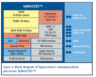
The soon-to-be-released hyNet32XS™ unifies all required elements of the Micro WebTarget board on one single chip. It integrates a RISC CPU, DSP, memory controller and 128 KByte SRAM together with communication interfaces such as UARTs, I2C, and Ethernet. Hyperstone integrates both the medium access control (MAC) as well as the physical layer (PHY) for a 10Mbit/second and a 100 Mbit/second Ethernet interface. The integration of MAC and PHY into a single chip is one of the unique features of the hyNet32XS (see Figure 4). The development of such a small and optimized SoC requires a very close technology partnership between suppliers of the processor and operating system. The combination of hyNet32XS and HyNetOS can truly be called an SoC, especially if additional Bluetooth™ IP's – such as the BOOST™ Core from Wireless IP Industry leader NewLogic – is integrated at a later stage.
Conclusion
Customers have access to all options under Hyperstone's flexible business model and developers may want to select their suppliers with the long-term vision of future SoC design projects in mind. The Hyperstone architecture is the best solution for many applications due to its combination of RISC and DSP as well as its ultimate power efficiency. Thanks to the small silicon footprint with only 35,000 gates (without RAM), the CPU macro cell is an inexpensive alternative for integration into SoC implementations. With a performance of up to 880 MOPS and low power consumption, the processor offers an efficiency of up to 3.6 GOPS per Watt. The DSP performance of 0.25 ms for a 1k complex FFT with 16-bit data easily measures up to dedicated DSP chips. Micro WebTarget™ and Micro BlueTarget™ are available now, and reference boards based on the hyNet32XS will be available in the second half of 2003 from both Hyperstone and SND.
Related Articles
- Stop-For-Top IP model to replace One-Stop-Shop by 2025... and support the creation of successful Chiplet business
- Gartner Says Semiconductor IP Companies Trying to Find the Business Model to Succeed
- Intellectual Property Reuse – A New Business Model
- Vendors debate viable IP business model
- Hardware/software codesign needs new business model
New Articles
- How to Design Secure SoCs: Essential Security Features for Digital Designers
- System level on-chip monitoring and analytics with Tessent Embedded Analytics
- What tamper detection IP brings to SoC designs
- RISC-V in 2025: Progress, Challenges,and What's Next for Automotive & OpenHardware
- Understanding MACsec and Its Integration
Most Popular
|
|
E-mail This Article |
|
Printer-Friendly Page |


