By Ram Niwas and Gaurav Kumar - eInfochips (An Arrow Company)
The Bandgap Reference (BGR) circuit is a key element in Very-large-scale Integration (VLSI) designs, providing a stable reference voltage that is crucial for the performance and reliability of analog and mixed-signal systems. This blog explores the design of BGR circuits in 90nm Complementary Metal-oxide-semiconductor (CMOS) technology by using Synopsys HSPICE, with a particular focus on transient analysis. It discusses the principles of BGR design, the challenges associated with scaling to 90nm, and the impact of transient behavior on the performance of VLSI systems.
As semiconductor technology continues to advance into deep submicron regions, the design of reliable analog components like BGR circuits faces increasing challenges. In 90nm CMOS technology, variations in temperature, power supply, and process parameters can significantly affect the performance of BGR circuits, making robust design practices essential. Transient analysis, which examines the circuit's response to changes in input and environmental conditions over time, is critical in ensuring that BGR circuits maintain their stability and accuracy. This blog provides a comprehensive overview of BGR circuit design in 90nm VLSI technology. It highlights the principles behind BGR operation, discusses the challenges posed by the 90nm process node, and emphasizes the importance of transient analysis in optimizing circuit performance.
Principles of Bandgap Reference Design
Fundamentals of Bandgap Reference Circuits
A Bandgap Reference circuit generates a stable output voltage that is largely independent of temperature, supply voltage, and process variations. The core idea is to combine two voltages with opposite temperature coefficients — Proportional to Absolute Temperature (PTAT) and Complementary to Absolute Temperature (CTAT) — in such a way that their temperature dependencies cancel out, resulting in a temperature-independent reference voltage.
BGR gives a temperature-independent reference voltage. Temperature independence can be obtained by combining two events with diametrically opposed temperature coefficients [6]. Because of this, Temperature Coefficient (TC) voltage and positive TC are combined to form the BGR reference voltage. For example, BGR is composed of CTAT and PTAT circuits that can compensate for each other and maintain a steady voltage regardless of temperature fluctuations.
CTAT may also be used in conjunction with an absolute thermometer. Fig.1 illustrates a CTAT graph where voltage is inversely proportional to temperature.
The output reference voltage Vref​ can be expressed as:

Where VBE​ is the base-emitter voltage with a CTAT characteristic and ∆VBE ​ is the difference in base-emitter voltages of two BJTs, providing a PTAT voltage.
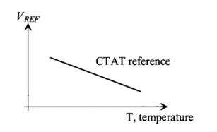
Figure 1: CTAT Graph (Voltage Versus Temperature)
PTAT, on the other hand, is accepted as a temperature-dependent constant. This relationship between voltage and temperature is shown in Figure2.
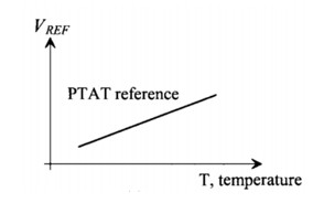
Figure 2: PTAT Graph (Voltage Versus Temperature)
According to Figure3, combining the PTAT and CTAT voltages results in a constant voltage over a range of temperatures.
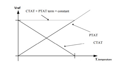
Figure 3: combination of PTAT and CTAT Graph
Transient Analysis of BGR Circuits
Importance of Transient Analysis
Transient analysis examines how a circuit responds over time to changes in inputs or environmental conditions, such as power supply variations or temperature changes. For BGR circuits, transient analysis is critical in ensuring that the reference voltage remains stable under dynamic conditions, such as power-up or sudden changes in load.
Transient Behavior in 90nm BGR Circuits
In 90nm technology, the transient response of BGR circuits can be affected by several factors, including parasitic capacitances, device mismatches, and supply noise. These factors can cause overshoot, undershoot, or ringing in the output voltage, which must be minimized to ensure reliable operation.
Simulation Techniques for Transient Analysis
To accurately model the transient behavior of BGR circuits in 90nm technology, advanced simulation tools such as Synopsys HSPICE are used. This tool allows simulating the circuit's response to various transient conditions, enabling the identification and mitigation of potential stability issues.
Key aspects to consider during transient analysis include:
- Power-up Response: Ensuring the BGR circuit settles quickly to the correct reference voltage with minimal overshoot or ringing.
- Load Transients: Analyzing how the circuit responds to sudden changes in load that can impact the stability of the reference voltage.
- Supply Voltage Fluctuations: Assessing the circuit's ability to reject noise or fluctuations in the supply voltage that is crucial to maintain accuracy in the reference output.
Simulation Results

Figure 4: Schematic diagram of BGR

Figure 5: Transient analysis of BGR

Figure 6: CTAT Graph (Voltage Versus Temperature)
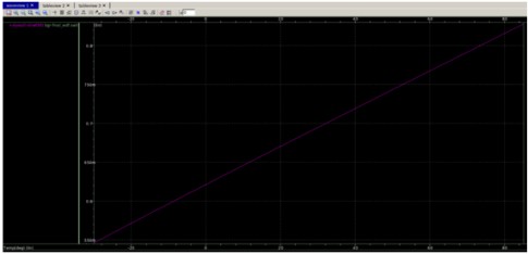
Figure 7: PTAT Graph (Voltage Versus Temperature)
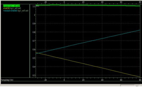
Figure 8: Combination of PTAT and CTAT Graph

Figure 9: DC analysis of BGR W.R.T. V source
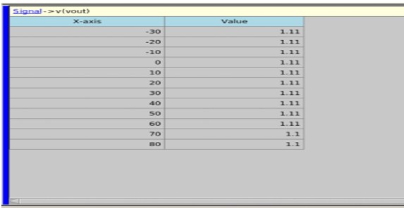
Figure 10: DC analysis of BGR W.R.T. temp
Challenges in 90nm BGR Design
Impact of Process Variations
In 90nm CMOS technology, process variations can lead to significant mismatches in transistor characteristics and resistor values, impacting the accuracy of the reference voltage. As the device dimensions shrink, these variations become more pronounced, making it challenging to achieve a stable output voltage.
Power Supply Sensitivity
The smaller geometries in 90nm technology make circuits more sensitive to supply voltage fluctuations. Ensuring a high-Power Supply Rejection Ratio (PSRR) in BGR circuits is essential to minimize the impact of these variations.
Leakage Currents
In deep submicron technologies like 90nm, leakage currents become a significant concern, especially in low-power designs. Leakage currents can introduce errors in the BGR output, affecting both accuracy and stability.
Applications of BGR Circuits in 90nm VLSI
BGR circuits are widely used in a range of VLSI applications, where a stable reference voltage is essential for reliable operation:
- Analog-to-Digital Converters (ADCs): BGR circuits provide a stable reference voltage,crucial for accurate analog-to-digital conversion.
- Digital-to-Analog Converters (DACs): In DACs, a stable reference voltage ensures the correct conversion of digital signals to analog outputs.
- Voltage Regulators: BGR circuits are used in voltage regulators to set precise output voltages, ensuring consistent performance across different operating conditions.
- On-Chip Temperature Sensors: BGR circuits provide a stable reference for temperature sensors, which is critical for accurate temperature measurement and compensation.
Conclusion
The design of Bandgap Reference circuits in 90nm VLSI technology presents unique challenges, particularly in managing process variations, power supply sensitivity, and transient behavior. Through careful design and analysis, including comprehensive transient analysis, it is possible to achieve stable and reliable BGR circuits that meet the stringent requirements of modern VLSI systems. As technology continues to scale, the principles and techniques discussed in this blog will remain essential for ensuring the performance and reliability of BGR circuits in increasingly complex VLSI designs.
References
- Razavi, B. (2000). Design of Analog CMOS Integrated Circuits. McGraw-Hill.
- Gray, P. R., Hurst, P. J., Lewis, S. H., & Meyer, R. G. (2009). Analysis and Design of Analog Integrated Circuits (5th ed.). Wiley.
- Allen, P. E., & Holberg, D. R. (2002). CMOS Analog Circuit Design (2nd ed.). Oxford University Press.
- Enz, C. C., & Temes, G. C. (1996). Circuit Techniques for Reducing the Effects of Op-Amp Imperfections: Autozeroing, Correlated Double Sampling, and Chopper Stabilization. Proceedings of the IEEE, 84(11), 1584-1614.
Authors Bio:
Author Name: Ram Niwas

Ram Niwas is a Senior Engineer at eInfochips (An Arrow Company). He completed his B. Tech in Electronics and Communication Engineering from Indraprastha Engineering College. With 6 years of experience in the VLSI domain, he has worked on several layout projects across various technology nodes, including 28nm, 45nm, 90nm, 130nm, and 180nm.
Author Name: Gaurav Kumar

Gaurav Kumar is an Engineer at eInfochips Pvt. Ltd., with over 2 years of experience in analog design and layout. He holds an M. Tech degree from GLA University, Mathura. Throughout his career, he has developed expertise in analog circuit design, layout techniques, and VLSI technologies. His contributions to the field of analog design have helped optimize performance and efficiency in various projects at eInfochips.
