Featured Article

This paper showcases the study on the Setup/Hold inter-dependence. It examines different existing methods for characterization and presents a new method to determine the Setup/Hold pairing for Standard Cells. This new method developed by Dolphin Integration is applied particularly on the pulsed latch (spinner system) in order to obtain the best compromise between circuit's speed and the reliability.
Featured Article
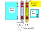
An Nor-type MLC ROM, Multi Layer Cell Read Only Memory macro of 16M bits (actual 32M bits) density is presented. The MLC ROM is designed by a 0.090 μm CMOS logic process. The ROM cell of 0.40μm ×0.50μm with 0.03μm per step of the channel width and channel length increase is determined to obtain 4 levels of Ids. A scheme of 2-step sensing with current-to-voltage converter (step1) and an ADC (step2) are applied to obtain an access time of 5 ns. 4 bits per cell can be achieved by inserting more referencing columns of ROM cells to track and to compensate noise from power and ground bouncing.
Featured Article

Consumer’s voracious appetite for quick access mobile content is obligating the need for high-resolution, high-speed data convertors in their mobile internet devices. Whether the transmission pipe is via cellular networks such as LTE or via local networks such as WiFi, the end requirement for the data convertor remains largely the same, those being higher bandwidth, higher speed, lower power and ownership costs that the consumer market can tolerate. This paper presents the key emerging market requirements for high-speed data-convertors, the metrics to use, and the architectural choices. It completes with a review of a highly efficient SAR ADC.
Featured Article
These days, there is a requirement of achieving high frequency targets with lower power consumption. Achieving both the targets simultaneously is very difficult and the situation becomes even more complex while moving down the technology nodes due to various sub-micron effects. With more features being integrated in modern SoC’s, the total number of gates used is increasing. Moreover higher throughput necessitates operating the design at higher frequencies. All this leads to significant increases in power consumption and die size. The proposed circuit is a single supply level shifter to translate the signal from one power domain to another power domain.