D&R Industry Articles (January 2017)
Articles for the Week of January 30, 2017

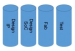
A Knowledge Sharing Framework for Fabs, SoC Design Houses and IP Vendors
The semiconductor industry has knowledge siloed into Design, Fab and Test. This paper proposes data structures specific to IP design characteristics for test manufacturing data system that can connect these silos. These structures enhance the ability to comprehend manufacturability at the IP level. Benefits for IDMs, Foundries, IP developers and System on a Chip (SoC) design houses are listed. Challenges in implementing these data structures in an IDM environment are included as well as data analysis examples.Articles for the Week of January 23, 2017

A Cost-Effective Reuse Method of Off-the-Shelf MIMO Wireless LAN IPs with a Nested Spatial Mapping
This paper presents a spatial mapping which turns dual data streams of MIMO system into an equivalent single stream. It is achieved by shrinking the constellation of the secondary stream into that of the primary data stream so that the primary one can be decoded even with a simple SISO de-mapper.- Electronic Circuit Design for RF Energy Harvesting using 28nm FD-SOI Technology
- Exploring a Parallel Universe - It's Coming to a Design Near You
Articles for the Week of January 16, 2017

Applying Continuous Integration to Hardware Design and Verification
With Agile approaches being applied with more or less success to hardware design and verification development processes, the question to apply a continuous integration flow in a hardware development process is raised.- Building low power into the system at the device driver leve
- Turning cars into mobile devices: MIPI
- Using FPGAs in Mobile Heterogeneous Computing Architectures
Articles for the Week of January 9, 2017

Design Considerations for High Bandwidth Memory Controller
High Bandwidth Memory (HBM) is a high-performance 3D-stacked DRAM. It is a technology which stacks up DRAM chips (memory die) vertically on a high speed logic layer which are connected by vertical interconnect technology called TSV (through silicon via) which reduces the connectivity impedance and thereby total power consumption.- Embedded FPGA: Changing the Way Chips Are Designed
- In Pursuit of Power
- Can we trust the cloud for video analytics?
Articles for the Week of January 2, 2017

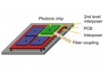
Rapid Physical Prototyping of Microelectronic Systems Based on Incompatible Technologies (The case for silicon interposers)
The market for Semiconductor Intellectual Property is well served for standard process technologies but not all functions are offered in all processes. Mixing and matching high performance digital CMOS, analog components, MEMS and optical devices can be an expensive and risky endeavour. Users often want to create a functional prototype for testing and sampling before committing to full production tooling or custom process development. Silicon Interposers can fill the gap by allowing users to mix and match components in different fabrication technologies with numerous advantages over Printed Circuit Board implementations.- Latch-Based RAMs and the Hidden Capacitor
- Understanding the Technology behind Traffic Sign Recognition (TSR) Systems


