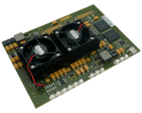
Gleichmann Research announces a 2-FPGA-Board with free partitioning software
Based on the ALTERA® EP2S180 in a 1508 pin package, Gleichmann Research offers a 2- FPGA-module for the Hpe®_midi systems. Every FPGA has 180.000 logic elements (equivalent to 1.8 Mio. ASIC gates). There are ~700 interconnections between the FPGA’s, 64 LVDS pairs allow 1Gbit/s/pair high-speed data communication. A 24-layer PCB, impedance controlled, temperature depended fan control and a clock factory, which distribute 7 input clocks to different clock inputs of the FPGA’s – these are some of the features of our FPGA development systems. We have also implemented the ALTERA® USB-Blaster™ on the module.
 Together with every FPGA-system we will deliver a set of software tools, which are easily accessible via a GUI, (Hpe®_desk). In addition to the clock factory the developer will receive a JTAG scanner and debugger. With this scriptable tool it’s possible to write any output and to read any input of the FPGA. In addition GE-Research offers to every customer, a cost-free, semi-automatic partitioning software. This allows the developer to move every entity from every level by dragging and dropping them into an FPGA. During this task the utilization and the interconnection will be checked. The partitioning tool is currently a beta-released version and works only with VHDL, but this will change within 2008. The tool needs only ALTERA Quartus®II, no additional expensive software will be required.
For more information go to: www.ge-research.com.
Gleichmann Electronics Research (Austria) Gmbh & Co KG
Gleichmann Electronics Research (Austria) GmbH & Co KG is a subsidiary company of Gleichmann & Co Electronics GmbH in Frankenthal (D). Founded in 2004 the company develops and manufactures development tools for FPGA’s (Field Programmable Gate Arrays) and offers services in connection with ASIC-development.
|
||||||
Related News
- Gidel FPGA boards used for next generation wireless communication research
- Faraday Launches SoReal! 2.0 Virtual Platform to Support Its FPGA Board for Early SoC Software Development
- Free Software Enables Development of IEEE 1149.1-2011 JTAG and IJTAG Based Infrastructure IP for FPGA and SoCs
- RIKEN adopts Siemens' emulation and High-Level Synthesis platforms for next-generation AI device research
- Samsung Collaborates With Arm To Drive Research in Software for Next-Generation Communication Technologies
Breaking News
- intoPIX Powers Ikegami's New IPX-100 with JPEG XS for Seamless & Low-Latency IP Production
- Tower Semiconductor and Alcyon Photonics Announce Collaboration to Accelerate Integrated Photonics Innovation
- Qualcomm initiates global anti-trust complaint about Arm
- EnSilica Agrees $18m 7 Year Design and Supply ASIC Contract
- SiliconIntervention Announces Availability of Silicon Based Fractal-D Audio Amplifier Evaluation Board
Most Popular
- Qualcomm initiates global anti-trust complaint about Arm
- Siemens acquires Altair to create most complete AI-powered portfolio of industrial software
- Alphawave Semi Reveals Suite of Optoelectronics Silicon Products addressing Hyperscaler Datacenter and AI Interconnect Market
- EnSilica Agrees $18m 7 Year Design and Supply ASIC Contract
- Rapidus Announces Strategic Partnership with Quest Global to Enable Advanced 2nm Solutions for the AI Chip Era
|
|
E-mail This Article |
|
Printer-Friendly Page |


