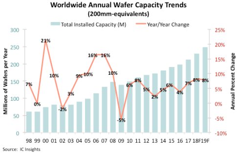
Wafer capacity growth of 8% forecast for 2018 and 2019 versus 4.8% average yearly growth from 2012-2017.
February 12, 2018 -- IC industry wafer capacity, specifically in the memory segment, was inadequate to meet demand throughout 2017. However, with Samsung, SK Hynix, Micron, Intel, Toshiba/WD, and XMC/Yangtze River Storage Technology planning to significantly ramp up 3D NAND flash capacity over the next few years, and Samsung and SK Hynix boosting DRAM capacity this year and next, what does this mean for total industry capacity growth? In its 2018-2022 Global Wafer Capacity report, IC Insights shows that new manufacturing lines are expected to boost industry capacity 8% in both 2018 and 2019 (Figure 1). From 2017-2022, annual growth in IC industry capacity is forecast to average 6.0% compared to 4.8% average growth from 2012-2017.

Figure 1
Large swings in the addition or contraction of wafer capacity by the industry, as a whole, appear to be moderating. Since 2010, annual changes in wafer capacity volume have been in the relatively narrow range of 2-8%, with the largest year-to-year difference being just three percentage points. This suggests that IC manufacturers are better today than in years past about trying to match supply with demand. It’s still an incredibly difficult task for companies to gauge how much capacity will be needed to meet demand from customers, especially given the time it takes a company to move from the decision to build a new fab to that fab being ready for mass production.
Many companies, DRAM and NAND flash suppliers in particular, have become much more active with new fab construction and expansion projects at existing fabs. This surge in activity comes after four years (2014-2017) when capacity growth lagged wafer start volume increases. During the past few years, IC producers have worked to increase utilization rates from the low levels in 2012-2013.
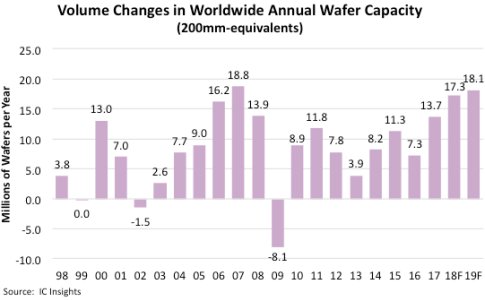
If all the new fab capacity expected to be brought on-line in 2019 happens as planned, the volume of capacity added that year will approach the record set in 2007. Figure 2 shows more that 18 million wafers per year of new capacity is expected to be added in 2019, and this number even assumes some of the massive DRAM and NAND fabs being built by Chinese companies will not be carried out quite as aggressively as has been advertised. IC Insights believes that construction of these China-owned fabs is progressing slower than planned.

Figure 2
Report Details: Global Wafer Capacity 2018-2022
IC Insights’ Global Wafer Capacity 2018-2022—Detailed Analysis and Forecast of the IC Industry’s Wafer Fab Capacity report assesses the IC industry’s capacity by wafer size, minimum process geometry, technology type, geographic region, and by device type through 2022. The report includes detailed profiles of the companies with the greatest fab capacity and gives comprehensive specifications on existing wafer fab facilities. Global Wafer Capacity 2018-2022 is priced at $4,490 for an individual user license. A multi-user worldwide corporate license is available for $7,190.
To review additional information about IC Insights’ new and existing market research reports and services please visit our website: www.icinsights.com.