10Gbps Multi-Protocol PHY IP
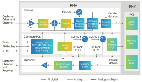
The PHY IP is designed to deliver high eye-margin at low power for backplane application. Numerous auto-calibrated circuits, programmable state machines throughout the design for PHY performance tuning, and the LC tank PLL provide low-power optimum performance.
View 10Gbps Multi-Protocol PHY IP full description to...
- see the entire 10Gbps Multi-Protocol PHY IP datasheet
- get in contact with 10Gbps Multi-Protocol PHY IP Supplier
Block Diagram of the 10Gbps Multi-Protocol PHY IP IP Core

Multi-protocol IP
- Multi-Protocol Crypto Packet Engine, Low Power, Bus Attached
- Multi-Protocol Crypto Engine
- Multi-Protocol Crypto Engine with Classification
- Multi-Protocol Engine with Classifier, Look-Aside, 5-10 Gbps
- Multi-protocol SerDes PMA - PCIe1 PCIe2 PCIe3 PCIe4 PCIe5 and more
- 1-56/112G Multi-protocol Serdes (Interlaken, JESD204, CPRI, Ethernet, OIF/CEI)


