Adaptive Clock Generation Module for DVFS and Droop Response
CSIX to PI40
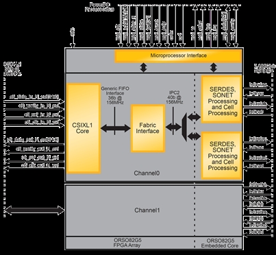
Lattice Semiconductor’s CSIX-to-PI40 core links a compliant CSIX-L1 interface to Lattice’s dual SERDES interface (compatible with PI40 interface). Inbound data frames from the CSIX port are deposited into the core's inbound FIFO. These CSIX frames are converted to PI40 cells and driven onto the dual SERDES interface. PI40 cells received on the dual SERDES interface are converted to CSIX frames and placed in the outbound FIFO. CSIX frames stored in the core's out-bound FIFOs are driven onto the outbound CSIX interface.
View CSIX to PI40 full description to...
- see the entire CSIX to PI40 datasheet
- get in contact with CSIX to PI40 Supplier
Block Diagram of the CSIX to PI40 IP Core

FPGA IP
- RT-630-FPGA Hardware Root of Trust Security Processor for Cloud/AI/ML SoC FIPS-140
- Complete USB Type-C Power Delivery PHY, RTL, and Software
- Ethernet TSN Switch IP Core - Efficient and Massively Customizable
- CXL 2.0 Agilex FPGA Acclerator Card
- PCIe Gen3 to SRIO Gen3 Bridge (FPGA)
- 65nm/40nm Low Power eFPGA IP and Open Source FPGA Software


