DDR3 PHY
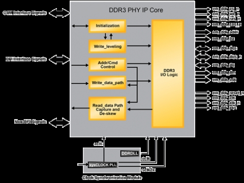
The DDR3 PHY IP reduces the effort required to integrate any DDR3 memory controller with Lattice FPGA’s DDR3 primitives and thereby enables the user to implement only the logical portion of the memory controller in the user design. The Lattice’s DDR3 PHY IP contains all the logics required for Memory device initialization procedure, Write leveling, Read data capture and Read data de-skew that are dependent on FPGA DDR IO primitives.
View DDR3 PHY full description to...
- see the entire DDR3 PHY datasheet
- get in contact with DDR3 PHY Supplier
Block Diagram of the DDR3 PHY IP Core

FPGA IP
- RT-630-FPGA Hardware Root of Trust Security Processor for Cloud/AI/ML SoC FIPS-140
- Complete USB Type-C Power Delivery PHY, RTL, and Software
- Ethernet TSN Switch IP Core - Efficient and Massively Customizable
- CXL 2.0 Agilex FPGA Acclerator Card
- PCIe Gen3 to SRIO Gen3 Bridge (FPGA)
- 65nm/40nm Low Power eFPGA IP and Open Source FPGA Software


