SD 4.0 UHS-II PHY in TSMC 40LP
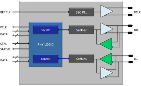
The UHS-II PHY IP is a comprehensive, silicon-proven configurable core that has been ported to multiple process nodes and leading foundries. It uses sub-LVDS signaling consisting of one pair each for transmit, receive and an additional reference clock. This low-pin count interface has reduced power consumption and low Electro Magnetic Interface (EMI). To further reduce power, the reference clock operates at 1/15th or 1/30th of the data transfer speed. This differential clock operates between 26MHz to 52 MHz and is carried over the legacy SD lines DAT0, and DAT1.
Arasan’s UHS-II PHY operates in both the Full-duplex and Half-duplex modes. It includes an 8b/10b encoder/decoder. The controller side of the interface of the UHS-II
PHY operates in the range between 39 Mbps to 156 Mbps. The default data lane D0 is used for downstream connection and the D1 lane is used for the other direction. An 8b/10b coding scheme is used. To improve testability, the UHS-II PHY implements the standard loopback paths.
View SD 4.0 UHS-II PHY in TSMC 40LP full description to...
- see the entire SD 4.0 UHS-II PHY in TSMC 40LP datasheet
- get in contact with SD 4.0 UHS-II PHY in TSMC 40LP Supplier
Block Diagram of the SD 4.0 UHS-II PHY in TSMC 40LP


