Video Frame Buffer
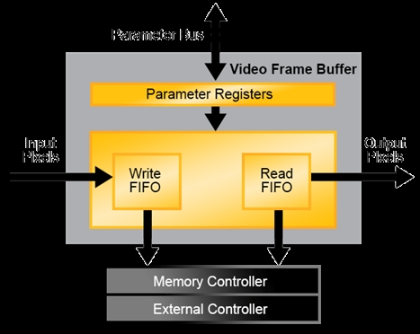
The Video Frame Buffer IP core receives input video data, stores it in the external memory and outputs it based on the timing controlled by the dout_enable signal. The core stores data into memory in a different width format as required by the application. It also provides synchronization of data across different clock domains as well as different format domains.
The core provides a simple parameter bus for dynamic frame size updating. It also implements a flexible memory interface that can be connected to Lattice memory controller IP cores.
The core also supports interlaced video stream by combining two fields into one frame outside.
The core supports continuous data streams from/to external interfaces in different clock domains using asynchronous Write and Read FIFOs. Input pixels are packed and stored into the asynchronous double clock Write FIFO first. Then pixels are sent to an external memory controller to be written to the memory. After an entire video frame has been stored in the external memory, frame reading starts. The pixels read from external memory are stored in the asynchronous Read FIFO and transferred to output interface clock domain. After unpacking, pixels are output from the Video Frame Buffer IP core.
In the video frame buffer, several clock sources are involved. The memory interface operates on a separate memory clock. When frame rate conversion is enabled, there are two clocks in the video data path: input pixel sample clock and output pixel sample clock. When frame rate conversion is disabled, the video data path oper-ates at input pixel sample clock rate. When dynamic parameter updating is enabled, the parameter bus can be configured to run on a separate clock. By default, the parameter bus runs on the input pixel sample clock.
View Video Frame Buffer full description to...
- see the entire Video Frame Buffer datasheet
- get in contact with Video Frame Buffer Supplier
Block Diagram of the Video Frame Buffer IP Core

FPGA IP
- RT-630-FPGA Hardware Root of Trust Security Processor for Cloud/AI/ML SoC FIPS-140
- Complete USB Type-C Power Delivery PHY, RTL, and Software
- Ethernet TSN Switch IP Core - Efficient and Massively Customizable
- CXL 2.0 Agilex FPGA Acclerator Card
- PCIe Gen3 to SRIO Gen3 Bridge (FPGA)
- 65nm/40nm Low Power eFPGA IP and Open Source FPGA Software


