Plano, TX USA
Abstract
The capacity and performance requirements of today’s complex digital systems often require the use of high-end Field Programmable Gate Arrays (FPGAs) or standard cell Application Specific Integrated Circuits (ASICs). Both solutions can meet most technical requirements but at what cost? High-end FPGAs extract exorbitant unit cost while standard cell ASICs have high upfront Non- Recurring Engineering (NRE) cost. In addition to project cost, performance and capacity issues, hardware designers must also overcome Time-To- Market (TTM) pressures, pay close attention to power budgets and maintain acceptable levels of risk. This paper discusses a FPGA to structured ASIC conversion methodology that will reduce cost, risk, TTM and power consumption while maintaining or increasing performance.
What is a Structured ASIC?
Simply put a structured ASIC, sometimes known as an array-based platform ASIC, is an ASIC where a large portion of the silicon is reused and customization is achieved via programmable metal layers. Reuse comes in the form of predefined, often embedded, IP.
A structured ASIC contains embedded IP that is both functionally verified and proven interoperable at the system level. The importance of proven interoperability cannot be overstated. With standard cell ASIC design even mature IP can cause problems when integrated into a new system. Structured ASICs resolve problems with integration by pre-verifying critical blocks at the system level. Therefore, when implementing the system, the designer has less to worry about in terms of performance, jitter and overall timing closure. Key embedded blocks used in almost all digital designs include timing generators (DLL/PLL), specialty IO (SSTL, LVDS, HSTL, LVPECL, etc.), physical interfaces or PHYs (DDR1/DDR2, PCI, Ethernet, etc.) and high-speed, feature-rich, block memories.
The overall effect of all this functionally proven, deterministically timed IP is less risk. And risk is the one thing that must be managed successfully with today’s designs.
Figure 1, shown below, illustrates the architecture of AMI Semiconductor’s XPressArray®-II structured ASIC.

Figure 1: XPressArray®-II Architecture
The IP, shown in Figure 1, is embedded in the base of XPressArray®-II, while the custom application is routed in the top few metal layers. This provides two key benefits of using a structured ASIC: reduced NRE and reduced development span. While these IP are critical components of every design, the impact of minimizing NRE and development span is felt the most if an Engineering Change Order (ECO) is required.
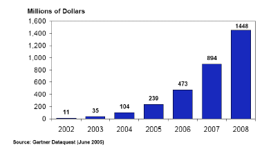
It is no surprise that as more designers learn about structured ASICs and the obvious technical and business benefits of using them in their designs that structured ASICs are starting to make a bigger splash in the market. According to Gartner
Dataquest, structured ASICs will grow from $100 million in 2004 to almost $1.5 billion in 2008. See Figure 2, shown below. That kind of projected revenue growth over a four year period is impressive and yields a Compound Annual Growth Rate (CAGR) of 93%.

Figure 2: Structured ASIC Revenue
Structured ASIC vs. FPGA
Now that we have defined what a structured ASIC is let’s see how it compares to FPGAs. To accomplish this comparison we are going to look at the different hardware platforms and see how they impact the primary design issues. The primary design issues, as previously noted, include cost, TTM, risk, performance, capacity and power
- Cost
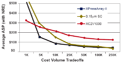
When discussing cost one must look at both Non- Recurring Engineering (NRE) costs and production costs to determine the overall cost effectiveness of the hardware platform. FPGAs have the lowest NRE but highest production cost. With FPGAs there are no reticles to buy but that does not mean they have zero NRE. The NRE for FPGAs is composed of the engineering cost associated with implementing the device. For FPGAs the bulk of the engineering effort is expended during place and route. With today’s high-performance systems, meeting timing closure in a FPGA can easily consume weeks if not months of engineering effort. High-end FPGAs have staggeringly high per unit cost. A top-of-the-line FPGA will easily exceed $1,000 per part, making them prohibitive for lifetime volumes exceeding five to ten thousand units.
With a per-unit cost up to 70% less than an equivalent FPGA and one fourth the NRE of a comparable standard cell ASIC, structured ASICs are a good fit for most mid-volume applications. The graph shown at the bottom of the page compares the average ASP cost over volume for a high-end FPGA, 0.15um standard cell ASIC and the XPressArray®-II structured ASIC (including NRE).

- Time-To-Market (TTM)
TTM is a critical issue for any development project. Failing to have the product ready at the start of the market window can cost a company a considerable amount of revenue. Missing the market window altogether can make the product worthless, costing the company its entire investment of time, resource and money spent developing the product. FPGAs offer the fastest TTM. Within two months of completing the design, the FPGA can be ready for production. Standard cell ASICs are on the other end of the spectrum, taking more than six months to reach production. Structured ASICs take longer than FPGAs to develop but less time than standard cell ASICs, since only a few metal layers need to be fabricated.
- Risk
With the complexity of digital circuits growing, ECOs are becoming more of the mainstream, instead of the exception. On average today’s designs are going through multiple ECO cycles. An ECO of an FPGA is relatively painless, at least in terms of hard currency. An ECO of a standard cell ASIC, on the other hand, can be extremely expensive, in terms of time, resource and money. Since an ECO can only affect the customizable portion of the structured ASIC, the impact to both span and NRE is considerably less than a standard cell ASIC.
- Performance & Capacity
As complex digital systems evolve, terms like bandwidth and bit rate take on greater importance. Designs within those systems need to squeeze out as much performance as possible. Structured ASIC technology provides the edge needed in performance over comparable FPGAs.
Field programmability comes at the price of reduced gate density. This means that for a given die area, structured ASICs will always offer a higher gate count than a FPGA. Giving the structured ASIC the edge over the FPGA when considering capacity.
- Power
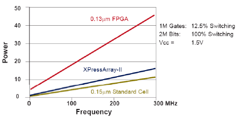
Power is also another critical resource in today’s complex digital systems. Handheld wireless devices are just one example. As handheld devices get smaller and smaller, the available power decreases while at the same time the complexity of the design increases. All this means that digital designs used in such devices must conserve as much power as possible. Current structured ASIC technology offers substantially less power consumption than FPGAs and is unequivocally the better choice for such applications. The graph at the bottom of the page compares the power consumption between a highend FPGA, 0.15um standard cell ASIC and the XPressArray®-II structured ASIC.

FPGA Prototyping to Structured ASIC Production
Initially using FPGA technology for proof-ofconcept by prototyping the design followed by an FPGA to structured ASIC conversion can greatly reduce overall cost, shorten TTM, reduce risk and maintain a high level of performance at moderate levels of power consumption.
By prototyping with a FPGA prior to committing the design to structured ASIC silicon, the risk of an ECO greatly impacting cost or development span is greatly mitigated. FPGA prototyping shortens the time from specification to hardware/software coverification. This is important because it supports the software team with real hardware for test and debug, versus hardware/software co-simulation or even hardware emulation. Co-simulation is extremely slow. In the case of today’s multi-million gate designs, co-simulation is lucky to achieve an equivalent simulation time of a few clock cycles of the system clock for every second of real time. Practically, this restricts software simulations to just a small portion of the overall design. Hardwarebased acceleration can be used to speed up the simulation; however, it is only geared to speeding up the DUT simulation in isolation and not at the system level. Hardware-base emulation does allow verification at the system level but it is an expensive solution that can only achieve speeds up to a few MHz. FPGA prototyping is an inexpensive way to verify software on real hardware at, or at least, close to full production speed. With the performance of today’s FPGAs, most designs can be prototyped “atspeedâ€, where at-speed refers to full production speeds. For bleeding edge designs that outpace what can be implemented in a modern FPGA, there is still enormous value in prototyping the design at reduced speed, to verify functionality.
Another concern with FPGA prototyping is capacity. Will the end design actually fit into the FPGA? Since the end product is a structured ASIC, designers do not need to worry overly much about the size of their design. If the design out grows a single FPGA, the design can be partitioned into multiple FPGAs for prototyping. Most FPGA vendors offer software that will enable automatic partitioning of the design. This either requires a daughter board or a separate board layout from the production version, but boards are relatively inexpensive in terms of both cost and man power.
While FPGA prototyping is highly recommended for functional and timing verification, it is not automatic. One must take care to design their product to support both FPGA and structured ASIC technology. In most cases this simply means following good design practices, such as avoiding latches, minimizing clock domains, crossing clock domains correctly when multiple clock domains are necessary and protecting the design against metastable conditions. However, there is one pitfall that is extremely easy to fall into: the use of proprietary IP. FPGA companies offer proprietary IP that cannot be ported across technologies, either due to technical or legal reasons. Often, this IP is sold for a whim or even given away. But watch out, this “free†IP can come with a hefty price tag, if it forces the design to stay in expensive FPGAs over volume production. AMI Semiconductor, the leader in FPGA conversions, has made it a point to offer cost effective IP solutions that, while optimized for structured ASIC technology, are also readily available for FPGA prototyping.
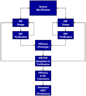
The following figure illustrates the FPGA prototype to structured ASIC methodology flow.

Figure 3: FPGA Prototype to SA Production
Since structured ASIC technology will be used for actual production in this methodology flow, performance and power are not even an issue. Structured ASICs have the edge in both performance and power by a substantial margin. This methodology will work for both low power and high performance applications.
Prototyping in a FPGA, then migrating to a Structured ASIC enhances the quality of the overall product. The designer not only has the option of lab testing the FPGA prototype but also the option of taking the FPGA to limited production, allowing the design to be fully tested out in the real world. After the design is mature, error free and the features are locked down, the design can be converted to a structured ASIC that is guaranteed to be functionally equivalent. The structured ASIC is then used in large scale production where SCAN and BIST are used to maintain manufacturing quality.
Conclusion
The perfect blend for most applications will be to prototype in FPGAs then convert that design to a structured ASIC for production. AMI Semiconductor’s XPressArray®-II structured ASIC was specifically designed to facilitate FPGA conversions. With FPGA compatible IO, timing generators, block memories and other IP, one can seamlessly prototype their design in an FPGA then migrate that design to XPressArray®-II for production.
Following this design paradigm will allow designers to take advantage of the benefits of using both FPGAs and structured ASICs without experiencing many of the drawbacks of either technology. The following table summarizes the advantages of this methodology flow versus the more traditional FPGA and standard cell ASIC production flows.

REFERENCES
[1] “EDA Vendors Should Keep Serving Both ASIC and FPGA Designersâ€; Gartner Dataquest; August 2005
[2] “FPGA-based Prototyping: Why All ASICs Should be Prototyped Using FPGAsâ€; Synplicity, Inc.; 2005
[3] “Systems-on-Chip for High-Speed Communication Systemsâ€; Synopsys, Inc.; 2002
[4] “XPressArray®-II Data Sheetâ€; AMI Semiconductor, Inc.; Revision 2.1; September 2005
[5] “Virtex-II Data Sheetâ€; Xilinx, Inc.; Version 3.4, March 2005;
