By Yuping Chung Arasan Chip Systems
Executive Summary
The explosive growth in portable devices over the past decade continues to challenge manufacturers wishing to add memory to their products that meet these four basic criteria:
- High bandwidth
- High capacity
- Low power
- Low cost
Flash storage technology and standards have evolved rapidly to meet these requirements. Universal Flash Storage (UFS) was created for mobile applications and computer systems requiring high performance and low power consumption. These systems typically use embedded Flash based on the JEDEC standard eMMC. UFS was defined by JEDEC as the evolutionary replacement for eMMC offering significantly higher memory bandwidth. The standard builds on existing standards such as the SCSI command set, the MIPI Alliance M-PHY and UniProSM as well as eMMC form factors to simplify adoption and development.
Arasan is actively supporting UFS IP solutions and development environment.
Introduction
Higher data transfer bandwidth requirements are driven by data traffic such as multimedia content download/upload and multi-threaded operations. Storage device have to maintain performance to support transfers of large multimedia files such as video, music and photos as well as actively running multiple applications on a mobile platform.
Accompanying the technology improvements have been standards developments that allow applications to use the storage interactively. The standards also have allowed applications to migrate from parallel bus interface to serial differential transmission for higher throughput and lower pin count.
Standard Bodies to the Rescue
As flash technologies have leapt forward, new interface standards have been developed to take advantage of them. An early entry to the standards scene was the SD Association, which supported only removable, large capacity cards for user content storage. The JEDEC standard eMMC, unlike SD offered bootable on-board storage for large code and application software as well as user content in a non-removable package. While eMMC continues to use a single ended bus interface, most other data storage interface standards have adopted serial differential signaling to meet the ever increasing high bandwidth requirements. In 2008 JEDEC began looking for a serial differential solution to replace eMMC.
A separate industry consortium, the Mobile Industry Processor Interface (MIPI) Alliances, also had an interest in developing a high-performance, serial I/O standard that could serve as a unified connection for data transfers between different processors and peripheral devices on a mobile platform, such as with camera sensors or display panels. One of the critical peripherals on a mobile device is the data storage device. MIPI was considering a data storage device to take advantage of its unified serial differential interface.
Un-divide and conquer
As both standards bodies were defining new specifications for the same peripherals, it became clear that there was a need for only one. In 2010, both MIPI and JEDEC adopted UFS as the common data transfer protocol for mobile systems.
Universal Flash Storage (UFS)
UFS uses a layered architecture as specified in JEDEC standard 220A. The upper layers in the standard were defined by the JEDEC while lower layers in the protocol where adopted from existing MIPI UniPro and M-PHY standards. Intended for applications requiring large storage capacity for data and bootable code, UFS offers a simple, but high-performance, serial interface that efficiently moves data between a host processor and mass storage devices.
Leverage the SCSI command set
The UFS standard adopts the well-known SCSI Architecture Model and command protocols supporting multiple commands with command queuing features and enabling a multi-threaded programming paradigm. This differs from conventional flash-based memory cards (eg eMMC) and embedded flash solutions which process one command at a time, limiting random read/write access performance.
In addition, a complementary UFS Host Controller Interface (HCI) specification allows system designers greater flexibility by simplifying the involvement of the host processor in the operation of the flash storage subsystem. The adoption of SCSI provides a well-known software- programming model and enables wider market adoption. It provides a standard programming interface for UFS by enabling the use of common Host/OS drivers and a common register set for the OS driver as well as a low-level driver, which can be customized as necessary for the HW host controller. It gives optimized support for various UFS usage models with regards to embedded mass storage memory card and UFS bus topology.
These specifications enable efficient transitions between the active and power save modes. Combined with a low active power level and a near-zero idle power level, UFS offers the promise for significant reductions in device power consumption. It will satiate the ever-growing demand for versatile storage solutions and improved device performance.
UFS provides for both embedded and removable card formats with the same interface, which simplifies controller design.
Time to market and low barriers to adoption
For the best reusability, UFS leverages existing standards of MIPI architecture and SCSI command sets. UFS adopted MIPI UniPro and M-PHY for the link and PHY layers, and the SCSI command sets as the application protocol. UFS uses serial interface for high-speed data transmission; it also implements power management to lower the power consumption.
Compatibility
UFS is an upcoming new mobile storage interface. But the challenge for an Application Processor (AP) SoC is to support multiple standards plus backward compatibility. SD has evolved from the single ended bus interface used in SD 3 to the differential serial transmission pairs. As an SoC designer, you will need to support the backward compatibility by implementing both singled ended and serial interfaces. Similarly, eMMC has also evolved from single data rate to double data rate in order to support 200MB/s bandwidth. Again, the SoC needs to be backward compatible.
Standard NAND Device Interface
One of the newer interfaces in mobile storage is the ONFI NAND interface. Again, it has evolved from ONFI 2.3 to ONFI 3.0 and the backward compatibility is very critical to the SoC designers.
To mitigate the challenges of backward compatibility, it is very important to choose a solution that offers the complete suite of IP components that address the design complexity, the standard compliances, and the interoperability among different devices. When choosing an IP provider, it is preferred to choose an IP certified by test centers, along with the associated analog IP and software drivers and utilities. In addition, ability to verify the IP before tape out and the ability to validate the 1st silicon in a hardware platform is also critical to shorten the development cycle.
UFS Architecture
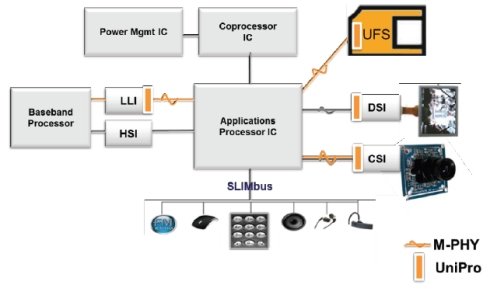
In a mobile device with a typical MIPI platform implementation, there are several different peripherals using the same physical interfaces (i.e. D-PHY or M-PHY) and the same link layer (i.e. UniPro).

Figure 1. UFS in a MIPI configuration
Peripherals using D-PHY or M-PHY include high bandwidth data storage interface (UFS), camera serial interface (CSI), display serial interface (DSI), and low latency interface (LLI). Using the same interface IP for multiple peripherals in a mobile device greatly simplifies the design effort and improves the time to market.
UFS Implementation Detail
In the diagram below, the implementation of a UFS host or device is simplified to the M-PHY, digital (UniPro) core and the interface to either the Soc or the NAND Flash memory. We will examine each of these in detail.

Figure 2. UFS to UFS Interface
UFS Layered Architecture
There are three major layers in the UFS architecture: UCS, UTP and Interconnect (UniPro + M-PHY). The command set layer (UCS) is the interface to the software application and incorporates the SCSI standard as the baseline protocol for UFS specification. The Transport Layer (UTP) is responsible for encapsulating the protocol into the appropriate frame structure for the interconnect layer. The Interconnect Layer (UIC) is a combination of digital and analog IP.
 4
4
Figure 3. UFS Layered Architecture
Let's take a look of what UniPro does. UniPro stands for Universal Protocol defined by MIPI. UniPro has four layers, L1.5 the PHY adapter, L2 the data link layer, L3, the network layer, and L4, the transport layer. Layer 1.5 and 2 ensures the data integrity and reliability, while layer 3 and 4 ensures the data is routed to the intended UFS host or device.
Layer 4 attaches the application data or message with header, trailer, and destination C-port to generate a segment. Layer 3 further attached the destination device information to the segment and it becomes a packet. Layer 2 adds the CRC to become a frame so the receiving end can verify the data integrity. Layer 1.5 and Layer 1 convert each frame to become encoded symbols before transmission to minimize the transmission errors and increase the transmission accuracy.
UniPro, if licensed from an IP vendor like Arasan, must first pass the certification program currently managed by University of New Hampshire. Since it is certified, this IP is provided virtually as a black box with standard interfaces to M-PHY on one side and to HCI or NAND controller on the other side.
M-PHY I/O
MIPI defines two types of M-PHY, type 1 and type 2. The UFS specification calls out type 1. M-PHY Type 1 uses NRZ signaling for HS and PWM signaling for LS, while type 2 uses NRZ signaling for both HS and LS.
UFS utilizes two speed modes, high-speed and low-speed. Low speed mode In Gear 1 is used upon power up or reset, then a transition occurs to high-speed gears for data transmission. The low speed gears and high-speed gears are listed here for your reference. UFS v1.1 has been ratified and supports HS Gear 2 running approximately @ 3Gbps per lane. The UFS spec also supports up to 4 lanes for higher throughput.
In order to conserve power and save battery life, M-PHY also supports multiple power states.
- Stall - HS
- Sleep - LS
- Hibern8 – configuration intact
- Disabled - configuration reset to default
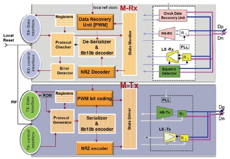
M-PHY Detailed Operation
The M-PHY performs several functions
1. Transmitter and Receiver
2. Squelch detection for power saving
3. 8b10 coding and encoding for signal balancing and data recovery
4. Serializer and de-serializer
5. Error detection

Figure 4. M-PHY Detail
The last element in a UFS device is the NAND Flash Memory and the corresponding controller.
Arasan Total IP Solution for UFS
In summary, a total IP solution for UFS requires digital IP for the UFS controller, including UniPro, the analog M-PHY, verification IP, software stack, and hardware validation platform.
- Analog M-PHY & ONFI Pads - Delivered as GDS-II for customer specific process technology, with on-chip testability, low power and small silicon area
- Digital IP UFS & NAND – Delivered as RTL along with verification IP and synthesis scripts. Consequently, the core is process independent, and designed for easy integration into your SoC
- Verification IP – Includes a Verilog simulation environment with a comprehensive test suite
- Software stacks – Includes bus interface layer, low level driver, protocol stack and API's to simplify peripheral or function driver development
- Hardware Validation Platform –
- A platform for evaluating devices & firmware.
- A platform for validating host controller implementation and interface to system bus.
- A platform for application software debug & analysis
- A platform for comparing SD/eMMC devices
References
1. UFS is defined by JEDEC – See http://jedec.org
2. UFS utilizes standards defined by MIPI – See http://mipi.org
3. UFS adoption is supported by UFSA – See http://universalflash.org
