by Gérard Boudon, John Fakiris *, Thibaud Besson, Véronique Guerre, Pierre Debord, Jacques Rota-Biesdorf, Christophe Delapchier, Didier Malcavet
IBM - 91105 Corbeil-Essonnes, France
*AMCC - ePPC Division- Cary NC, USA
Abstract
The Design of a PowerPC system-on-a-chip processor which integrates high speed state of the art 800 MHz PowerPC IP, DDRII-667 memory controller, RAID assist logic, and three PCI-X DDR266 interfaces with a rich mix of conventional peripherals is described. The PowerPC, with on-chip L2 cache enabled, executes up to 1600 DMIPS. The RAID assist logic is capable of transferring 2 Gbytes/sec. The state of the art PowerPC, the high bandwidth data pipes, and the RAID assist logic make the SOC an ideal solution for RAID controller applications. Active power consumption is as low as 6W with a 1.5 volt supply. The SOC has been implemented in a 0.13 um, 1.5 V nominal-supply, bulk CMOS process.
I-INTRODUCTION
This PowerPC system-on-a-chip (SOC) design platform is intended to address the high-performance RAID market segment. The SOC uses IBM’s Core-Connect technology [1] to integrate a rich set of features including a DDRII-667 SDRAM controller, three PCI-X DDR266 interfaces, hardware accelerated XOR, I2O messaging, three DMA controllers, a 1Gb Ethernet port, a parallel peripheral Bus, three UARTs, general purpose IO, general purpose timers, and two IIC buses.
- CMOS 0.13 um Copper
- 7 levels of Metal
- 11.757 million gates
- Gate area = 3x12 channels of 0.4um
- 29mm FC-PBGA (Flip chip Plastic Ball Grid Array)
- 1mm pitch
- 528 Signal I/Os
- 783 Pads
II- SYSTEM OVERVIEW
This SOC design consists of a high performance 32-bit RISC processor core, which is fully compliant with the PowerPC specification. The processor core for this design is based upon an existing, fixed voltage PowerPC 440 core [2]. The core includes a hardware multiply accumulate unit, static branch prediction support, and a 64-entry, fully-associative translation look aside buffer. The CPU pipeline is seven stages deep. Single cycle access, 64-way set associative, 32- KByte instruction and data caches are connected to the processor core.
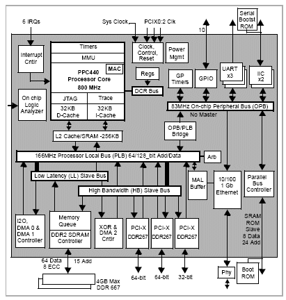
Figure 1 SOC IOP processor block diagram
A second level (L2) cache of 256 KB is integrated to improve processor performance. Applications that do not require L2 may optionally use the L2 as on chip SRAM. The L2 memory arrays include redundant bits for parity and spares that can be connected after test and configured with on chip fuses.
III ACHITECTURE: CROSSBAR PLB BUS
The key element of this SOC for high speed data transfer is the central 128b wide 167 MHz crossbar PLB (Processor Local Bus) [1]. Two out of eleven masters can simultaneously access one of the two PLB slave buses: one specialized in High Bandwidth(HB) data transfer and a second one with Low Latency (LL). The same physical memory in the SDRAM can be accessed either on the HB or the LL slave bus through two aliased address ranges. By convention (but not required) the LL bus segment is used by the PowerPC to achieve low latency access to memory while the HB bus segment is used by the large data movers such as the DMA engines. The Crossbar architecture separates the 64b address, 128b read data, and the 128b write data busses allowing simultaneously duplex operations per master with two independent masters resulting in a peak theoretical bandwidth of 10 Gbytes/sec.
While the Crossbar arbiter supports 64 bit addressing, the PowerPC440 CPU is a 32 bit processor that can address up to 4 GB of physical address. The 64 entry TLB transforms this address to a real 36 bit PLB address (upper 28 bits are 0s) for 64GB access of the total address space.
IV Memory Controller / DDRII-667
The integrated memory controller supports both DDRI and DDRII SDRAM in 64-bit or 32-bit configurations with optional ECC and is dual-ported with separate system interfaces to distinguish quality of service. The Low Latency (LL) port implements smaller data buffers and is optimized for Low Latency access while the High Bandwidth (HB) port has larger data buffers and is optimized for maximum throughput. Memory accesses through the LL segment may optionally be programmed to have higher priority than those of the HB segment, effectively allowing the LL requests to move ahead of HB requests within the memory read/write queue.
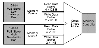
Figure 2: Memory Controller Queue block diagram
Automatic self-refresh entry is provided to support RAID battery-backed caches. In the event reset is asserted the memory is automatically placed in self-refresh to preserve the memory contents. Power may be removed from the SOC as long as the memory is supplied power from an alternate source. The memory is kept in self-refresh until specifically instructed to come out of self-refresh by the PowerPC.
DDR I and DDR II SDRAM are supported through a flexible, fully programmable timing interface. In addition to programmable command and interface timings, the memory controller supports a fine grained, phase advance/delay mechanism to enable Clock/Data/DQS and DM interface timing adjustment and incorporates a digital DLL to enable process, voltage, and temperature compensation. The following table lists the supported DDR1 and DDR2 features:
| DDRII SDRAM | DDRI SDRAM | |
| Clock Freq | 200/266/333MHz | 100/133/166/200MHz |
| CMD Timing | Programmable | Programmable |
| Init. Sequence | Programmable | Programmable |
| Interface Width | 32/40-bit 64/72-bit | 32/40-bit 64/72-bit |
| 40-bit | ECC SEC/DED per Word | SEC/DED per Word |
| 72-bit | ECC SEC/DED per DWord | SEC/DED per DWord |
| Burst Length | 4 | 4 |
| Data Strobe | Differential/Single Ended | Single Ended |
| Supply Voltage | 1.8V | 2.5V |
| O Interface | SSTL_18 | SSTL_2 |
| New Functions | - ODT (On Die Termination) - OCD (Off-Chip Driver) calibration - Posted CAS - AL (Additive Latency) | |
V - Hardware XOR
The Hardware XOR engine computes a bit-wise XOR on up to 16 data streams with the results stored in a designated target. The XOR engine is driven by a linked list Command Block structure specifying control information, source operands, target operand, status information, and next link. Source and target can reside anywhere in PLB and/or PCI address space.
VI - I2O Messaging
The I2O messaging unit provides 2 messaging queues (i.e. 4 FIFOs) similar to what is defined in the I2O version 1.5 specification. In addition to the functions defined by the standard, the I2O messaging unit provides hardware to automatically move a message from the host to the SOC as a result of a messaging queue update without PowerPC involvement and supports 64 bit message frame addressing.
VII - DMA Engines (2)
The 2 DMA engines are high performance data movers drive by Command Block structures. Each DMA engine can independently do source to target data move, source to two target data move, target pattern fill, source pattern check, target LFSR fill, and source LFSR check. Source and target can reside anywhere in PLB and/or PCI address space and have any byte alignment
VIII - PCI-X DDR 267
Traditional PCI is a multidrop type of bus which limits its performance. The PCI-X DDR 267 mode 2 [5] is an evolution to a point to point bus while maintaining compliance with legacy PCI. The PCI-X 267 mode 2 introduces a DDR scheme to double the performance to up to 2 Gbytes/sec for a 64 bit bus.
Among the new features of the PCI-X mode 2 are DDR, ECC, and OCD control. The circuit of figure 3 that controls the impedance of the Off chip driver is based on the comparison of a group of NFETs in parallel with an external calibration resistance in a first step. The adjustment is done by turning on/off several NFETs. In a second step when NFETs are calibrated, the PFET impedance is compared to the NFET which should be equal to the external Resistance. The result of On/off PFET/NFET is applied to the final FET’s of the Off chip driver.
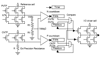
Figure 3: OCD Off-Chip Driver control circuit for PCI-X DDR mode 2
Miscellaneous Peripherals
The SOC includes all the standard peripherals required for a RAID controller including a 1Gb Ethernet port, a 83 MHz parallel peripheral Bus (up to 3 devices), three UARTs, general purpose IO, general purpose timers, and two 400 KHz master/slave capable IIC buses
IX - CLOCK DOMAINS
The combination of various cores such as a 800MHz CPU, three PCI-X DDR266 and a DDRII-667 SDRAM controller on a single SOC leads to the implementation of five (5) PLLs.
To generate the multiple high frequency clocks required by the SOC, two PLLs were cascaded to generate the CPU, memory Controller, and peripheral clocks. The CPU PLL drives the CPU and related peripherals while the DDR PLL is used exclusively to generate the 1X and 2X clocks for the memory controller. Memory and CPU are synchronous and the clocking is built from the same external low frequency system clock. The DDR PLL input is driven by the PLB clock (generated by the CPU PLL).
To minimize the cumulative skew effects of non-adjacent cascaded PLLs the feedback of the DDR PLL is at the END of the clock tree it drives, effectively removing the delay of its input clock from the CPU PLL. This scheme can support the 2 PLL’s in each corner of the die inside their respective cores.
There are 3 independent PCI clocks inputs, one for each PCI-X interfaces with a PLL that generates a 2X internal PCI clock for the DDR mode. The PCI CLock domains and the PLB clock domain are completely asynchronous. A Request/Acknowledge handshake protocol was preferred to a two stages - double latch - synchronizer only solution for data transfer between PLB bus and External PCI agents. This design approach eliminates hazard and minimized latch metastability problems.
X - POWER DISSIPATION
The PowerPC architecture is well reputed for its low power dissipation coupled with high performance.
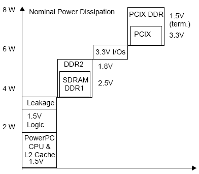
Figure 4: Power dissipation breakdown
The power breakdown of the various cores on the chip highlights the growing importance of the Memory controller and PCI-X busses at high frequency.
XI-IMPLEMENTATION
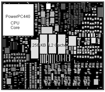
Figure 5: Chip layout showing I/O circuits - PLL and DLL’s, all SRAMs
Due to the large number of I/O (783) needed to integrate all the peripherals, the I/Os are placed in an area array across the die. A peripheral approach for IO implementation was possible with a staggered structure; however, it would have resulted in a larger die size, and a more noise sensitive part because of large simultaneous switching.
The device is based on an ASIC with integrated synthesizable cores - also named IP’s - with the exception of the PowerPC CPU core which is a precharacterized hard core with optimized timing analysis and tuned clock distribution to achieve 800MHz. By comparison the same CPU core runs only at 600MHz if implemented as a soft core with the best optimization tools.
Logic is described in Verilog and synthesis done with Synopsys synthesis tool. The physical design including floorplaning, placement and wiring was done with IBM’s proprietary Chip Bench tool. Special care was taken in physical implementation for minimization of noise induced by coupling and simultaneous switching on top of the conventional signal integrity verification.
Extensive simulation of each core with simulation after SOC integration has resulted in a first pass good product.
XII- TEST RESULTS
A special board with modular approach for PCI-X, DIMMS, and peripheral attachments has been developed. It permits the debug of the SOC device with DDR1 and DDR2 SDRAM as well as PCI, PCI-X and PCI-X DDR connectors. Debug was done with the Riscwatch debugger through the JTAG serial link I/O.
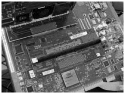
Figure 6: Board used for debug with DDR2 DIMMS close to the IOP processor and PCI-X bus analyzer
CONCLUSION
A SOC integrating a PowerPC CPU core with a large number of state of the art and conventional peripherals has been designed and tested good on its first pass of silicon. The CPU has been tested at 667Mhz and main interfaces such as DDRII SDRAM at 667MHz and PCI-X DDR mode 2 at 266MHz.
REFERENCES
[1] IBM Corp. (1999) Coreconnect Bus Architecture, Hopewell Junction, NY. [Online]. Available: http://www.chips.ibm.com/techlib/techlib.nsf/productfamilies/CoreConnect_Bus_Architecture
[2] IBM Corp.. (2000) PowerPC Embedded Cores, Hopewell Junction, NY. [Online]. Available: http://www.chips.ibm.com/techlib/techlib.nsf/products/PowerPC_440_Embedded_Cores
[3] JEDEC STANDARD DDR2 SDRAM SPECIFICATION (Revision of JESD79-2) January 2004
[4]W.Lau “Overcoming DDR-2 interface challenges†EDN, Jan 22, 2004
[5] PCI-X Addendum to the PCI Local Bus Specification, Version 2.0
