Triad Semiconductor, Inc.
Introduction
As the minimum feature size of semiconductor processes shrink, tooling costs escalate. Moreover, smaller minimum feature size leads to higher gate counts. Consequently, full-custom designs using smaller geometry processes (< 0.25 micron) cost more and take longer to design. It is difficult, for even the largest companies, to justify investment in a large full-custom ASIC. Structured ASICs are gaining in popularity because of this.
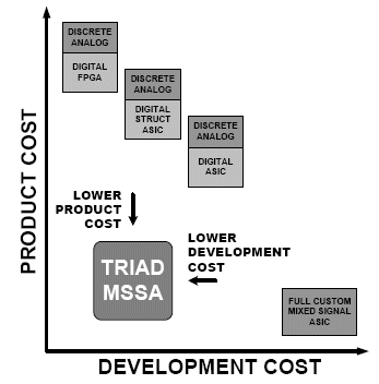
To date, structured ASICs have been primarily digital—analog has largely been ignored. Analog IC design has long been considered “full-custom only.†Triad Semiconductor's mixed signal structured arrays (MSSAs) facilitate the development of custom solutions for a fraction of the cost and development time, see Figure 1, when compared to typical full-custom ASICs.

Figure 1: ASIC Product cost vs. development cost.
In this presentation, we will introduce mixed signal/analog structured ASICs (MSSAs) as a means for resolving many of the issues confronting mixed signal IC designers—cycle time and tooling cost. We will show how Mentor Graphics’ and ViASIC’s IC EDA tools play a vital role in the MSSA design flow.
Structured ASICs
A structured ASIC is defined as any ASIC configured using less than all layers of metal. Commercial devices range from configuration of all but one metal layer, to configuring only a single via layer.
The benefits of structured ASICs come from having fewer custom masks per design, allowing reticles to be shared between designs. Naturally, these benefits are maximized when the number of custom reticles is minimum, or exactly one. A via layer is superior to a metal layer for this purpose for two reasons. First, vias connecting between layers do not block tracks above or below, enabling maximum channel signal widths. Second, via mask layers can be made more quickly, since only a small fraction of vias are actually used in any design, dramatically reducing the total line length that must be drawn on the reticle.
The idea of via-configurable Structured ASICs has been around at least since the late 1980's [1]. A significant barrier to these devices moving to large-scale production has been the lack of commercial software place and route tools. By their nature, via-configured ASICs cannot share the same router as cell based ASICs. However, ViaPathTM, developed by ViASIC, now provides a complete place and route tool optimized specifically for via-configurable devices.
Mixed Signal Structured ASICs
The technology behind the MSSA is similar to popular digital structured arrays; however, the MSSA includes via-configurable analog as well as digital.
The digital portion of the MSSA follows an FPGA like design flow. In other words, with a Verilog HDL netlist the digital section can be completely configured. A library of IP blocks including USB, SPI and microcontroller cores make it practical to implement entire embedded systems on-chip.
Differentiating the MSSA from digital structured arrays and FPGAs is the inclusion of analog. The analog section is composed of analog tiles. The analog tile is typically made up of OTAs, output buffers, resistors, capacitors, analog switches and clock generation/control logic. This facilitates the creation of a wide variety of analog functions such as gain stages, filters and sigma delta modulators. Since the analog elements that make up the analog tile are completely characterized, the user is able to work at a higher level without being burdened by designing all the underlying primitive cells. Designs that typically take several months can now be completed in weeks.
Triad Semiconductor's patent pending MSSA architecture is based on the ViaMask technology developed for digital structured arrays by ViASIC. Figure 2 shows a floor plan for a typical MSSA platform containing 12 analog tiles (A TILE), 4 analog I/O amplifiers (I/O OAs), 27 logic tiles (40 k gates + 6.9 kbytes of RAM) and 18 kbytes of via-configurable ROM.

Figure 2: MSSA floor plan.
Key Features of MSSA Technology
- Reduced development time
- Lower cost
- Mixed signal ASIC with true precision analog capability
- FPGA like design flow
In a nutshell, MSSA technology allows one to create high performance semi-custom ASICs by only modifying the VIA layer between metal 2 and metal 3. To develop an ASIC using an MSSA, the designer does not have to be familiar with all the intricate details of mixed signal IC design, only how they want their circuit/system configured.
MSSA Design Flow
The MSSA design flow shown in Figure 3 allows for entry at virtually any point in the development process. In other words, a customer can specify a turnkey ASIC or actually manipulate the physical via location or anywhere in between. A design can be prototyped in field programmable devices and off-the-shelf-components. When the prototype is verified it can be converted to an MSSA with minimal modification.

Figure 3: MSSA design flow.
It should be noted, the MSSA design flow is absent of layout (polygon editing) and layout verification (DRC and LVS). This is due to the fact that the MSSA platform has already been completely verified prior to production release. Hence, the MSSA designer is able to focus on design capture and simulation.
Analog Tile
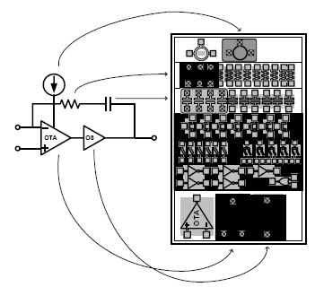
The analog tile is the macro building block in the analog portion of an MSSA. Figure 4 shows an example of an analog tile containing two operational transconductance amplifiers (OTAs), a buffer amplifier (OS), resistors, capacitors, switches and clock related circuits.

Figure 4: Analog Tile.
Notice the analog tile shown in Figure 4 does not contain an opamp. OTAs are excellent for switched capacitor circuits or wherever there is no resistive loading. When required, an opamp can be formed by cascading an OTA with an output stage (OS) as shown in Figure 5.

Figure 5: Analog tile used to make an opamp.
Analog Macro Models
To facilitate rapid full-chip simulation with ADMS, macro models are used for the OTAs and OS. The key parameters in an OTA macro model include small-signal voltage gain and frequency response with one dominant and one parasitic pole as well as small-signal input and output impedances, common-mode gain, and output voltage swing limiting.
In the Eldo (SPICE) macro model, shown in Figure 6, current sources (Norton equivalent source modeling) are used for gain stages as opposed to voltage sources (Thevenin equivalent source modeling) to reduce the number of circuit nodes used. This reduces the simulation solution time and overall complexity of circuit netlists.

Figure 6: OTA macro model.
Logic Tile
The digital portion of an MSSA is composed of logic tiles that are composed of logic cells. An example of a typical logic cell contains four NAND gates, two muxes, one D-type flip-flop and ten inverters as shown in Figure 7. A single logic cell is equivalent to approximately 11 gates.

Figure 7: Logic cell.
A logic tile contains 128 logic cells and 256 bytes of single port SRAM. The MSSA shown earlier in Figure 2 contains 27 logic tiles giving a total of approximately 38 k gates.
Mixed Signal Example
A switched capacitor filter is a simple example of a mixed signal circuit. MSSA technology is an excellent fit for this type of circuit. Figure 8 shows how a single analog tile can be used to implement a single switched capacitor biquadratic filter section. To make higher order filters, multiple analog tiles can be cascaded.
In the implementation of the filter section in Figure 8, not all the available elements are used. Hence, these are available to create other circuits or can be used in conjunction with another analog tile if necessary.
The clocks required for the switched capacitor filter would be generated in the digital section of the MSSA. Typically switched capacitor filters require two-phase non-overlapping clocks. Hence, the analog tile contains some logic, which can be used to generate the multiple phases locally. This keeps the number of signals that must be run from the digital section in to the analog section to a minimum.

Figure 8: Switched capacitor filter.
Summary
In this paper, we have introduced the mixed signal structured array (MSSA) as a means to cost effectively realize semi-custom mixed signal ASICs. We have shown how the MSSA EDA tool flow eliminates time consuming aspects of mixed signal development like polygon editing and layout verification.
References
1. Xilinx, Inc., San Jose, California. “Xilinx Hard Wire Data Bookâ€, 1991.
2. B. Cox, P. Dewell, D. Mavis, P. Eaton, and J. Kemerling “One-Mask Structured ASIC Technology for Cost Effective Radiation Hardened ICs,†GOMAC Tech, 2005.
3. Triad Semiconductor, Inc., http://www.triadsemi.com.
