This paper describes the implementation differences of an IP core between FPGA and RapidChip® Platform ASIC technologies. By mapping the same complex, high-speed PCI Express core onto these two technologies, a clear picture of relative merits can be observed.
SMALLER FOOTPRINT
A typical 8-lane (32Gbps aggregate) PCI Express interface can be implemented with a 64-bit data path running at 250MHz or with a 128-bit data path running at 125MHz. It is extremely difficult to successfully implement any reasonably complicated digital design (with ~20 logic levels) at 150MHz in FPGA technology. Reaching anywhere near 250MHz for such designs is not possible, even with the latest 90nm FPGAs. Therefore an x8 PCI Express core implemented in an FPGA will require a 128-bit datapath clocked at 125MHz.
By contrast, when implemented in RapidChip technology, the same core can easily achieve 250MHz allowing the smaller, more efficient 64-bit datapath implementation to be used. Due to its wider datapath, the FPGA implementation uses approximately 60% more logic resources than the RapidChip Platform ASIC implementation.
REDUCED LATENCY
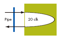
The latency of a controller greatly influences the overall performance of the PCI Express interface and thus the entire system. The round trip latency of a design is a very important metric. It is measured from the PIPE Rx to the PIPE Tx, going across the physical, link and transaction layers. A typical PCI Express controller configuration will have ~15- 25 clock cycle round trip latency.

Figure 1. Approximate device latency from packet received (no payload) to credit release
Consider the case of a controller with 20 clock cycles round trip latency. When implemented at 125MHz in an FPGA, the 20-clock cycle latency is 20x8ns = 160ns. The same core implemented at 250MHz in RapidChip technology has only 20x4ns = 80ns clock cycle latency. The 100% additional latency suffered by an FPGA implementation is a major reason for the superior performance of a RapidChip Platform ASIC.
BETTER LINK UTILIZATION
The reduced latency of RapidChip technology vs. an FPGA can also translate into in superior link utilization.
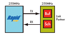
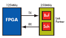
For example, consider the utilization of a PCI Express egress link with a standard- cell ASIC link-partner, in an Intel north bridge system. Figure 2a shows the PCI Express transmit path implemented in RapidChip technology. Figure 2b shows the PCI Express transmit path implemented in an FPGA.

Figure 2a. RapidChip Platform ASIC implementation 64-bit 250MHz

Figure 2b. FPGA implementation 128-bit 125MHz
In the transmit datapath, the PCI Express core sends packets to the standard link partner buffer. When packets leave this buffer, credits are released back to the PCI Express core.
The size of the receive buffer in the link partner and the latency in receiving the credit back to the PCI Express core determines how efficiently the link is utilized.
The fixed size of the Virtual Channel (VC) buffer on the receiving standardcell ASIC link partner will typically be optimized with the expectation of connection to a similar standard-cell ASIC like device. Thus it will work most efficiently when connected to something with corresponding latency similar to that of a standard-cell ASIC.
If the end-to-end latency involved in sending a packet from the PCI Express core and receiving the credit back is much more than the typical number assumed in the above buffer size estimation then the link will start idling due to credit starvation. This starvation occurs when the receiving buffer is not large enough to absorb the additional end-toend latency.
A simple comparison between the RapidChip Platform ASIC and FPGA implementations is shown in Figures 2c and 2d. This analysis is simplified by excluding the effects of packet size, credit release policy etc. Figure 2c shows how the RapidChip Platform ASIC implementation continuously sends packets.

Figure 2c. Link utilization of RapidChip Platform ASIC implementation

Figure 2d. Link utilization of FPGA implementation
Its ASIC-like latency allows credits to be received back fast enough to avoid starvation. In contrast Figure 2d shows how an FPGA has to wait much longer for credit updates to occur causing the link to go idle.
This example only considers the case of posted-write packet types, although the effects also apply to other packet types and multi-VC cases.
A major component of the credit latency path is the controller’s internal delay. Lets assume the round trip latency inside the link-partner is 20 cycles (at 250MHz). The most significant portion of the endto- end credit return delay is the sum of the round trip latencies of the both controllers. I.e. 20 x 4 ns for the link-partner plus 20 x 4ns for the RapidChip Platform ASIC implemented PCI Express core. This gives a total of 160ns. The same setup for an FPGA implementation of the PCI Express core will take 20 x 4 ns for the link-partner plus 20 x 8ns for the FPGA, giving a total of 240ns.
If the buffer in the link-partner has been designed to cover only the first case latency of 160ns, then the link utilization for the FPGA implementation will be 33% lower.
REDUCED BUFFER SIZE
The receive path to a PCI Express core also has similar link utilization considerations. In an FPGA implementation, the receive VC buffer size must be increased by 50% to absorb the increase in endto- end latency (240ns instead of 160ns, for the above example). This means the RapidChip Platform ASIC implementation requires a reduced buffer size compared with an FPGA implementation. If the FPGA receive buffer size is not increased, the receive path into the PCI Express core will also suffer from utilization problems.
INCREASED OVERALL PERFORMANCE
In addition to the local credit starvation and link utilization issues, the increased latency of an FPGA implementation affects other areas of system performance. Figures 3a and 3b highlight how latency affects the read performance in a system. For a given number of outstanding reads from a node, any increased latency in receiving a response adds significant waiting time for the read initiator. This reduces overall read bandwidth. If the read data contains assembly code to be executed or data-packets to be processed, then the efficiency of such processes will also be significantly reduced.

Figure 3a. Read request of RapidChip Platform ASIC implementation

Figure 3b. Read request of FPGA implementation
CONCLUSION
For complex and high-speed applications such as PCI Express, even the fastest 90nm FPGAs lack sufficient performance. This speed disadvantage can ultimately slow down the entire system.
The ASIC-like performance of RapidChip Platform ASIC on the other hand provides a clear performance advantage. This is especially important when connecting to standard cell ASIC link partner that assumes it will be connected to a lowlatency partner.
ACKNOWLEDGEMENT
We would like to thank GDA Technologies for their help in creating this white paper.
