Peter Woo, Senior Director of Product Marketing
eASIC Corp.
Moore’s Law Only for the Brave?
The costs and risks of designing custom silicon are putting innovation out of reach for all but the very bold. Ironically, Moore’s Law which forecasts predictable evolution towards finer and finer process geometries makes the technology accessible only for those with guts of steel. A “Law†that on one hand is driven by the market’s insatiable appetite for performance and cost efficiency, and on the other hand requires:

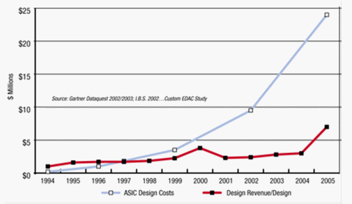
Figure 1: ASIC Costs Rising Faster Than Revenue
Figure 1 illustrates that ASIC costs are dramatically outpacing associated revenues, making their current development model prohibitive as a solution for anything but the surest of business opportunities.
ASIC Masks - The Key Culprit
Exorbitant and growing ASIC mask costs require customers to engage in extensive and expensive verification. Designers can expect a full 90 nm mask set to cost $1M, but this is only a small portion of the estimated ~$25M development cost of an ASIC. About half of the overall ~$25M is devoted to verification tools and engineering intended to increase the likelihood that silicon “works right, first time†and to avoid spending an indeterminate amount of time on analysis and money on masks. Unfortunately a majority of ASIC designs today require re-spins, as shown in Figure 2.
This $1M mask costs will be incurred whether the customer requires only 10 devices for prototyping/experimentation or 1 million devices for mass production. Therefore, customers can not embark on an ASIC project unless they are willing to invest the time and money to ensure the masks will be used to produce 100K’s of devices. Frankly, there are few opportunities today that, with absolute certainty, will require 500,000 units to provide a justifiable return on investment.

Figure 2: ASIC Re-Spins
Additionally, silicon foundries are universally moving to 300 mm wafers (from 200 mm) to lower device costs. Since foundries have a minimum number of wafers required for a manufacturing run, and more devices per wafer are manufactured on 300 mm wafers, the minimum number of devices required for a single order increases. Each ASIC purchase transaction needs to be in the 1K’s or even 10K’s of units depending on the complexity of the device. The prospect of signing up for 10,000 units and committing to $1M before seeing any silicon is daunting for even the most experienced designers.
One way to minimize this risk is to simply take an existing and well-understood ASIC in an established market and “tweak†it for the new process. But this limits innovation to be merely incremental. To support revolutionary innovation, a methodology involving a silicon prototype that is easy to modify is required. The primary perpetrator for a re-spin by a wide-margin is “Functional Logic Errorâ€, shown in Figure 3. Fortunately, this precise issue can be addressed with a prototype. Once the silicon prototype is functionally confirmed, only then does the customer commit to the larger volumes.

Figure 3: Reasons for ASIC Re-spins
Enter… Structured ASICs With Fewer Custom Masks
Large NREs and minimum order quantities with no ability to prototype have always plagued ASICs, but these problems become more acute at the finer process geometries. FPGAs address some of these problems, but their performance and cost shortcomings created an opportunity for a category of devices know as structured ASICs. As opposed to standard cell ASICs which require a new, complete mask set for each design, structured ASICs consist of a pre-fabricated, common base array containing logic, memory, and other diffused IP designed to serve multiple customers. Customization occurs on only the top layers, thus requiring only a handful of custom masks. Fewer masks lead to lower NREs and faster manufacturing times.
A Maskless Structured ASIC?
The ideal solution would be a structured ASIC that requires no masks up-front when the project’s technical and business merits are most uncertain. Without masks the barriers to access the technology will be lowered dramatically and customers could engage easily in innovation.
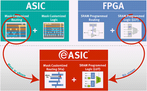
Today’s structured ASICs require the customization of two separate elements – logic and routing. An approach to reducing mask count could be to customize the routing and leave the logic to be programmable. eASIC has developed an approach that combines programmable SRAM LUT-based logic cells with efficient customized metal routing. Design logic is “softâ€, implemented using programmable SRAM-based look-up tables (LUTs), as in an FPGA, and customized by means of a bit-stream loaded at device power-up. The interconnect is “hardâ€, and like an ASIC is very fast, but once customized can not be altered. Note Figure 4.

Figure 4: Configurable LUTs + Mask Customized Interconnect
No NRE… Possible Through Technology, Not Subsidy
Routing is customized through a single via layer at the foundry, and is implemented quickly and inexpensively with an alternative lithography approach: the Direct-Write eBeam. The routing fabric consists of four layers of metal of varying lengths and directions. These tracks provide all the routing and can be customized with a single customized via layer. Note Figure 5. Since this single customized layer is printed directly on a wafer with eBeam technology, there is no need for a mask. No mask means no NRE.

Figure 5: Single Layer of Via Customization
No NRE provides maximum flexibility to innovate as customers can continue to modify designs without any concern over needing to salvage a large “sunk cost†associated with an incurred NRE. Other vendors that offer “No NRE†are most likely amortizing it over a large volume of devices, so any design changes will obligate the customer to commit to higher and higher unit volumes stifling risk-taking and innovation.
No Minimum Order Quantities… Go to High-Volume When It’s Right for You
Directly writing the via layer onto the wafer with eBeam allows the printing of different patterns directly onto the same wafer. Since multiple customer designs can be put on the same wafer with eBeam, customers do not need to commit to an entire wafer of devices. Note Figure 6. Customers order just the number of devices they need.

Figure 6: eBeam Enables Multiple Designs on Single Wafer
In the early stages of development where design changes to silicon are certain, the flexibility of being able to order just the number of devices required is important. No customer wants to be in a position of committing to thousands devices, making a design change, and then being forced to scrap thousands of useless devices.
Once the customer goes to high volume, eASIC will create a mask for absolute lowest cost, but no mask is required in the initial stage. Moreover, this mask is created late in the development process, as opposed to other structured ASIC solutions which need to make the mask (and incur the costs) right away. An eASIC customer can ship initially with eBeam manufactured devices, collect technical and market feedback, and then decide to go to a mask after the eBeam devices assure him that no design issues exist and high-volumes are certain. The same data file submitted for eBeam customization is later used for mask creation.
Powerful Prototypes Eliminate Risk
Virtually all ASIC designs today need to prototyped and the most powerful prototyping solutions are 1) available quickly, 2) straightforward to modify, and 3) identical to the production device. FPGA prototyping only satisfies the first two points. In fact, eASIC’s solution is unique in providing a maskless prototype that is identical to the mass production device, thereby introducing a great deal of risk when converting the prototype device to production.
Consider a structured ASIC solution where the prototypes are created with eBeam and production devices with a single mask. These devices are manufactured quickly since they are prefabricated up to the top layers and customized with a single layer. Other structured ASICs require about a half-dozen customized layers resulting in longer processing times as each layer requires about two days to process. eBeam devices are easy and inexpensive to modify since initial designs are customized without a mask. Finally, the prototype and production devices are the same. The underlying base silicon layers are identical; the only difference is the customization process. The high-volume production device uses a mask created from the same GDSII database used to direct the eBeam during prototype manufacturing. Note Figure 7.

Figure 7: Manufacturing Flow for Prototype and Production Device
Enabling Low-Risk Innovation
A no-mask, structured ASIC addresses the specific pain points in the ASIC design flow – high-upfront costs, large commitment requirement and unprecedented design risk. ASIC design starts are at a low indicating that innovation is stalling. This new innovative approach to custom silicon design enables powerful risk management and puts the power of innovation within everyone’s reach.
eASIC Corp.
Moore’s Law Only for the Brave?
The costs and risks of designing custom silicon are putting innovation out of reach for all but the very bold. Ironically, Moore’s Law which forecasts predictable evolution towards finer and finer process geometries makes the technology accessible only for those with guts of steel. A “Law†that on one hand is driven by the market’s insatiable appetite for performance and cost efficiency, and on the other hand requires:
- $1M - 2M mask expenditures upfront when the project’s payoff is most uncertain
- Large, upfront order commitments driven by increasing wafer sizes
- Long verification cycles to minimize chances of crippling design errors

Figure 1: ASIC Costs Rising Faster Than Revenue
Figure 1 illustrates that ASIC costs are dramatically outpacing associated revenues, making their current development model prohibitive as a solution for anything but the surest of business opportunities.
ASIC Masks - The Key Culprit
Exorbitant and growing ASIC mask costs require customers to engage in extensive and expensive verification. Designers can expect a full 90 nm mask set to cost $1M, but this is only a small portion of the estimated ~$25M development cost of an ASIC. About half of the overall ~$25M is devoted to verification tools and engineering intended to increase the likelihood that silicon “works right, first time†and to avoid spending an indeterminate amount of time on analysis and money on masks. Unfortunately a majority of ASIC designs today require re-spins, as shown in Figure 2.
This $1M mask costs will be incurred whether the customer requires only 10 devices for prototyping/experimentation or 1 million devices for mass production. Therefore, customers can not embark on an ASIC project unless they are willing to invest the time and money to ensure the masks will be used to produce 100K’s of devices. Frankly, there are few opportunities today that, with absolute certainty, will require 500,000 units to provide a justifiable return on investment.

Figure 2: ASIC Re-Spins
Additionally, silicon foundries are universally moving to 300 mm wafers (from 200 mm) to lower device costs. Since foundries have a minimum number of wafers required for a manufacturing run, and more devices per wafer are manufactured on 300 mm wafers, the minimum number of devices required for a single order increases. Each ASIC purchase transaction needs to be in the 1K’s or even 10K’s of units depending on the complexity of the device. The prospect of signing up for 10,000 units and committing to $1M before seeing any silicon is daunting for even the most experienced designers.
One way to minimize this risk is to simply take an existing and well-understood ASIC in an established market and “tweak†it for the new process. But this limits innovation to be merely incremental. To support revolutionary innovation, a methodology involving a silicon prototype that is easy to modify is required. The primary perpetrator for a re-spin by a wide-margin is “Functional Logic Errorâ€, shown in Figure 3. Fortunately, this precise issue can be addressed with a prototype. Once the silicon prototype is functionally confirmed, only then does the customer commit to the larger volumes.

Figure 3: Reasons for ASIC Re-spins
Enter… Structured ASICs With Fewer Custom Masks
Large NREs and minimum order quantities with no ability to prototype have always plagued ASICs, but these problems become more acute at the finer process geometries. FPGAs address some of these problems, but their performance and cost shortcomings created an opportunity for a category of devices know as structured ASICs. As opposed to standard cell ASICs which require a new, complete mask set for each design, structured ASICs consist of a pre-fabricated, common base array containing logic, memory, and other diffused IP designed to serve multiple customers. Customization occurs on only the top layers, thus requiring only a handful of custom masks. Fewer masks lead to lower NREs and faster manufacturing times.
A Maskless Structured ASIC?
The ideal solution would be a structured ASIC that requires no masks up-front when the project’s technical and business merits are most uncertain. Without masks the barriers to access the technology will be lowered dramatically and customers could engage easily in innovation.
Today’s structured ASICs require the customization of two separate elements – logic and routing. An approach to reducing mask count could be to customize the routing and leave the logic to be programmable. eASIC has developed an approach that combines programmable SRAM LUT-based logic cells with efficient customized metal routing. Design logic is “softâ€, implemented using programmable SRAM-based look-up tables (LUTs), as in an FPGA, and customized by means of a bit-stream loaded at device power-up. The interconnect is “hardâ€, and like an ASIC is very fast, but once customized can not be altered. Note Figure 4.

Figure 4: Configurable LUTs + Mask Customized Interconnect
No NRE… Possible Through Technology, Not Subsidy
Routing is customized through a single via layer at the foundry, and is implemented quickly and inexpensively with an alternative lithography approach: the Direct-Write eBeam. The routing fabric consists of four layers of metal of varying lengths and directions. These tracks provide all the routing and can be customized with a single customized via layer. Note Figure 5. Since this single customized layer is printed directly on a wafer with eBeam technology, there is no need for a mask. No mask means no NRE.

Figure 5: Single Layer of Via Customization
No NRE provides maximum flexibility to innovate as customers can continue to modify designs without any concern over needing to salvage a large “sunk cost†associated with an incurred NRE. Other vendors that offer “No NRE†are most likely amortizing it over a large volume of devices, so any design changes will obligate the customer to commit to higher and higher unit volumes stifling risk-taking and innovation.
No Minimum Order Quantities… Go to High-Volume When It’s Right for You
Directly writing the via layer onto the wafer with eBeam allows the printing of different patterns directly onto the same wafer. Since multiple customer designs can be put on the same wafer with eBeam, customers do not need to commit to an entire wafer of devices. Note Figure 6. Customers order just the number of devices they need.

Figure 6: eBeam Enables Multiple Designs on Single Wafer
In the early stages of development where design changes to silicon are certain, the flexibility of being able to order just the number of devices required is important. No customer wants to be in a position of committing to thousands devices, making a design change, and then being forced to scrap thousands of useless devices.
Once the customer goes to high volume, eASIC will create a mask for absolute lowest cost, but no mask is required in the initial stage. Moreover, this mask is created late in the development process, as opposed to other structured ASIC solutions which need to make the mask (and incur the costs) right away. An eASIC customer can ship initially with eBeam manufactured devices, collect technical and market feedback, and then decide to go to a mask after the eBeam devices assure him that no design issues exist and high-volumes are certain. The same data file submitted for eBeam customization is later used for mask creation.
Powerful Prototypes Eliminate Risk
Virtually all ASIC designs today need to prototyped and the most powerful prototyping solutions are 1) available quickly, 2) straightforward to modify, and 3) identical to the production device. FPGA prototyping only satisfies the first two points. In fact, eASIC’s solution is unique in providing a maskless prototype that is identical to the mass production device, thereby introducing a great deal of risk when converting the prototype device to production.
Consider a structured ASIC solution where the prototypes are created with eBeam and production devices with a single mask. These devices are manufactured quickly since they are prefabricated up to the top layers and customized with a single layer. Other structured ASICs require about a half-dozen customized layers resulting in longer processing times as each layer requires about two days to process. eBeam devices are easy and inexpensive to modify since initial designs are customized without a mask. Finally, the prototype and production devices are the same. The underlying base silicon layers are identical; the only difference is the customization process. The high-volume production device uses a mask created from the same GDSII database used to direct the eBeam during prototype manufacturing. Note Figure 7.

Figure 7: Manufacturing Flow for Prototype and Production Device
Enabling Low-Risk Innovation
A no-mask, structured ASIC addresses the specific pain points in the ASIC design flow – high-upfront costs, large commitment requirement and unprecedented design risk. ASIC design starts are at a low indicating that innovation is stalling. This new innovative approach to custom silicon design enables powerful risk management and puts the power of innovation within everyone’s reach.
