By Dr. Ramon Acosta, Nascentric, Inc
The demand to deliver faster, smaller, portable and more powerful wireless products is what drives the electronics market. Every visit to the local electronics store surprises us with a plethora of consumer electronics that change the way we live and communicate. Portable home healthcare electronics include a wearable non-invasive glucose monitor for diabetics, an in-home hemodialysis unit, and do-it-yourself screening tests for conditions ranging from high cholesterol to blood-borne infections. Today’s cell phones offer movie downloads and remote programming of home electronics that allow consumers to record television shows. To be successful in the marketplace, these mobile devices must match consumer demands. They must have many technically advanced features, perform instantaneously and be extremely small and inexpensive.
Satisfying these demands constantly impacts engineering schedules, strains limited engineering resources and interjects unpredictable costs into development budgets. To accelerate engineering schedules, minimize engineering resources and better manage development costs, many semiconductor manufacturers integrate third-party IP into their designs. The availability of robust IP alleviates a significant amount of pressure from the design teams; and its extensive usage in today’s large SoCs is a standing testament to its industry-wide appeal.
However, the close interaction between blocks in large SoCs makes it absolutely necessary to test functionally in each of the blocks separately while ensuring that these blocks interoperate flawlessly when connected.
The functional interaction between the interfaces is complex at best, requiring lengthy verification tests. IP blocks purchased from third-party vendors often need to be verified within the entire context of the chip rather late in the design cycle. Limited verification resources frequently inhibit the design teams ability to perform the comprehensive simulation and verification that is crucial for silicon success. In the midst of this new complexity, the chip integration team may not be aware of the intricacies of some blocks and may miss some small, yet crucial, functionality tests. To address some of these issues, the industry generally employs two methodologies for the design of large and complex chips; top-down and bottom-up.
Top-Down Methodology
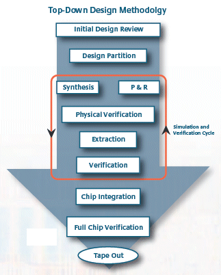
The more prevalent methodology of the two is the top-down approach (see Fig. 1). The tools supporting this design flow are robust, mature, highly automated and the issues are well understood. Commonly referred to as “Big D, Little a†designs, these architecture- driven designs mainly include digital blocks with a small amount of analog content. Designers using this methodology are familiar with HDLs such as Verilog and VHDL, and are comfortable using them in their design.
These designers generally focus on the functional view and do not concern themselves with a SPICElevel view of the analog block. A well-defined interface, such as the Open Core Protocol (OCP), helps them integrate the digital side IP blocks into the larger design. This methodology provides greater accommodation for changes to the design specification later in the design cycle. Proponents of this methodology then require a fast, high capacity, mixed-signal simulator to help functionally verify the digital/analog interface.

Fig. 1: Top-Down Methodology
Bottom-Up Methodology
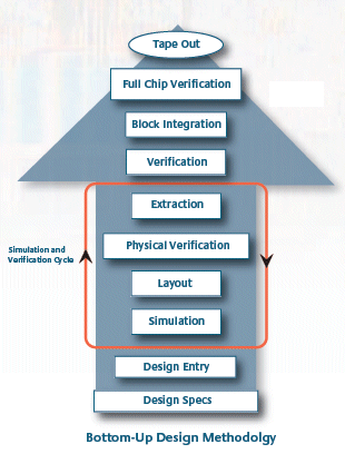
With the increase of mixed signal content in SoC designs, the bottom-up methodology (see Fig. 2) is becoming more prominent. These designs are typically block-driven “Big A, Little d†designs. While there are very mature point-tools, the design flow itself is very patchy and the level of integration is poor. Issues with the digital/analog blocks are quite complex and have more frequent analog content. Designers are very familiar with the SPICE-level view of the functional block yet they remain highly skeptical of any abstraction above the SPICE level. The functionality of designs is tested at every stage of the design cycle and when a problem is encountered at the top level, the integration/design team is typically responsible for diagnosing and fixing the problem.

Fig. 2: Bottom-Up Methodology
Design teams adopt popular formats such as OCP to help seamlessly integrate their IP blocks. The design cycles for bottom-up methodologies tend be long and rather inflexible to accommodating design specification changes late in the development cycle. In this case, designers require a fast, accurate mixed-signal simulator to help simulate large designs with greater accuracy.
Each of these methodologies provide significant structure to design teams but their successes are still dependent on the specifics of the design adoption. It is apparent that the availability of a fast, accurate, high-capacity, mixed-signal simulator remains a critical factor for success in either methodology. Design and verification teams have stoically employed traditional SPICE and Fast SPICE solutions to address their needs for these mixed signal designs. However, this approach has worked well for small functional analog and digital blocks, but fails for larger scale mixedsignal designs. There are several reasons for this:
- The traditional SPICE and Fast SPICE solutions primarily use voltage-based device models to predict the behavior of analog circuits. This works well for small stand-alone designs since the requirements on simulation capacity are small and performance is not as critical. Using a similar approach proves to be highly inefficient for large mixed-signal designs.
- The move to nanometer processes has introduced several physical effects that require a better understanding of the current flow through critical nodes. Traditional SPICE and Fast SPICE engines can determine this value, but only at great computational expense or by compromising accuracy.
- The traditional solutions employ one or two type(s) of simulation engine(s). As mixed-signal designs have multiple functional blocks with unique circuit and interconnect behavior, the 1 (or 2) simulation engine approach severely limits the performance and accuracy.
- When using SPICE/Fast SPICE solutions with voltage-based models, designers are given the option of either accuracy OR performance. This has proven to be a barrier for mixed-signal designers whose analog IP blocks requiregreater simulation accuracy; whereas digital blocks need better performance and larger capacity. Since both blocks need to be simulated together the trade-off presents a ‘no-win’selection.
- The nature of the mixed-signal blocks requires multiple concurrent analyses (such as detailed power analysis, grid analysis, etc.) to be performed while still checking for functionality and timing. Existing SPICE/Fast SPICE solutions are either too limited on capacity or too inaccurate to perform these types of functionality checks.
These issues have been long since noted throughout the analog IP/ mixed-signal design community which has clamored for a next generation simulation/verification solution for mixed-signal SOC designs for some time. To create a next-generation Fast SPICE simulation and verification solution one must begin by thinking out of the box. For example, Nascentric’s Nascim is a significant departure from the traditional SPICE and Fast SPICE approach to simulation, as it adopts a current-based transistor and interconnect model approach. The basic presumption is that active MOS devices are current-based devices, rather than voltage-based. By adopting the current-based approach, Nascim overcomes the key short-comings of traditional voltage-based solutions and provides a fast, accurate, high capacity simulation and verification capability. Additionally, it features innovative schemes that accurately capture the complex interconnect behavior and account for the greater part of signal loading. Multiple dedicated simulation engines combined with intelligent event-based simulation will accelerate the simulation/verification time. Customer trials have demonstrated speed-ups of 2X-10X run time improvements as compared with existing Fast-SPICE simulation and verification solutions while maintaining equal or better accuracy.
Successful development and implementation of third party IP is integral to meeting a design’s feature, schedule, performance, size and cost objectives. Adopting standards such as OCP are paramount in integrating verified combination of analog and digital blocks. Implementation of the IP blocks needs a strong foundation integration standard and requires that boundary conditions be well understood and fully characterized. By performing simulations more quickly and ensuring more robust verification coverage, next-generation simulation solutions will bring relief from much of the pain currently experienced in older simulation and verification approaches.
Dr. Ramon Acosta, V.P. of Engineering at Nascentric, is guiding the development Nascim, the next-generation Fast SPICE simulation tool.
