Livingston , Scotland
Abstract:
Verification has become the biggest challenge for companies developing IP and SoC products targeted at standards based specifications. For technologies, such as PCI Express and USB, compliance and interoperability testing at plug-fests or using accredited third party test facilities is now considered a requirement for success in the market place.
This has created a critical need for structured and coherent verification methodologies which take compliance and interoperability testing into account early and throughout the development process. Further the complexity of modern standards creates an enormous verification challenge which can only be met through the application of advanced verification techniques and optimal reuse. On top of this many applications for standards based interfaces need to carry out software / hardware co-design. For example graphics controllers need to integrate high performance wireline interfaces into massively complex SoCs, support co-design and meet ever shortening development cycles.
The availability of verification methodologies which are customised to the requirements of a particular standard is of great benefit when preparing for compliance testing while minimizing development timescales. In developing IP and providing SoC design services for customers Cadence are uniquely placed to understand this verification challenge. We have experience of optimising our verification methodology to take maximum advantage of powerful EDA software features, as well as utilising Cadence and partner hardware to enjoy the benefits of simulation acceleration, in-circuit emulation and protocol analysis.
This paper will describe the best use of software and hardware tools combined with verification IP in a multi-layered verification methodology as applied to real designs – in this case targeted at PCI Express applications. Through these examples it will highlight to developers the benefits available from incorporating a combination of transaction based RTL simulation, e Verification Components (eVCs), Palladium based emulation, prototyping and the use of protocol analysis tools.
Introduction
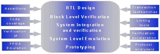
The diagram below highlights the rich variety of solutions which are available to enable developers to both accelerate and improve the quality of SoC verification. Each solution is discussed below and then a case study is used to examine how these were used successfully in the verification methodology of a silicon-proven design.
PSL Assertions
Property Specification Language (PSL) assertions may be used to aid the verification of complex designs both at block and system level. The assertions are embedded into RTL as comments meaning that they are invisible to tools not supporting PSL. In their simplest form PSL assertions may be used to monitor various signals for legal and illegal transitions (e.g. read and write for RAM not active simultaneously or illegal state machine transition) The assertions are understood by dynamic simulators such as ncsim. There are also tools available such as Incisive Formal Verifier from Cadence which will perform static analysis on PSL assertions. In dynamic mode the simulator can be made to report on the number of times specific assertions have been triggered and also pass/fail counts for each one. Since PSL assertions are embedded within RTL they are transportable between block level and system level verification without the need for any additional coding.
A further use for PSL assertions is they can allow members of a design team to specify and deliver interface information for block interconnects and protocols at an early stage of the design cycle. This helps minimise the chances of failure during top-level verification due to differing interpretations of ambiguous specifications.
Transaction based testbench
Traditional behavioural testbenches can become cumbersome and unwieldy as the complexity of designs grow. During system level verification, transaction based testbenches provide a greater level of abstraction by generating complete communication packets or entire read/write cycles across bus architectures. Generally these testbenches can be controlled via steering files written in pseudo code or some form of higher level language thus allowing the designer to target complex functional areas.
Code Coverage and lint
Linting tools are used in analysis of the RTL design and report language specific problems which could have an effect during synthesis. They are programmed using design rules specific to a company to ensure that designers produce more readable and re-useable code.
Code coverage provides an indication of the effectiveness of the testing performed on specific blocks within the whole design. By examining the code coverage logs it is easy to see where the holes in verification appear. These logs will indicate branches, statements or blocks where particular sections of the code have not been exercised at all. By examining the coverage logs the designer can write tests specifically to target those areas not covered.
Verification IP
Verification IP has a number of uses, in Cadence we have used this on PCI Express projects. The IP may be used in testbenches purely as a monitor to keep track of traffic across an interface and report on any violations with respect to existing standards or specifications. Another use is to use the verification IP as the basis for a testbench , with the IP behaving as initiator or target. Tests written for use with verification IP may be directed and aimed at specific spec points or compliance matrix entries, although in some cases a degree of randomness is possible. eVCs are different an eVC is natively random in nature. With an eVC, once the component has been configured correctly it will drive the interface with random packets/data and provides functional coverage information. This allows for greater coverage more quickly before having to resort to writing more directed tests.
Verification Acceleration
Verification acceleration systems, such as the Palladium from Cadence, may be used for vector debug and analysis, simulation acceleration or for emulation. Palladium provides access to the DUT’s I/O to the real world. SpeedBridge hardware, which buffers data transfers between the DUT and the real word, makes it possible to test software or firmware in a real system before going to silicon or even prior to use on an FPGA.
FPGA emulation
An FPGA board can help in working through final problems and multiple iterative builds of a design and is as representative as possible without having to commit to final silicon with all the NRE costs involved. The advantages of using FPGA over an acceleration system is that the design will run at full speed (or a close approximation ) and timing issues may be found or fixed . Also the design can be plugged into a real system to help in testing interoperability.
FPGA emulation is particularly useful for Compliance Workshop testing as it readily supports RTL changes to fix problems found in testing.
Protocol analysis
There are a number of different protocol analysers available for a wide range of standards, and with varying features. Analysers may be used as passive monitors being plugged in-circuit between an initiator and a target, or alternatively they may be used to initiate traffic as an exerciser or to receive traffic as an endpoint. We have found the passive and exerciser modes to be the most useful since our design efforts have always been targeted towards endpoints. In passive mode the analyser will perform in the same way as verification IP connected as a monitor in a testbench. The analyser keeps track of the traffic over the interface being tested and reports on any protocol violations.
In exerciser mode, the analyser may be used to drive the interface and so can be useful for reading config spaces, memory locations etc.
Case Study
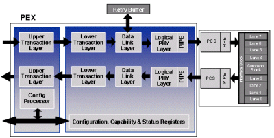
The above diagram shows the Cadence Design Systems PCI Express IP core. This case study shall examine the design of this core and highlight the use of the various verification techniques previously described. The end goal of the project was to take the Cadence PCI Express core to the PCI SIG Compliance Workshop, pass compliance testing and get the IP core added to the SIG’s Integrators List. Cadence act as the exclusive EDA reseller for Rambus PHYs and we made use of the Rambus PCI Express PHY test board as our compliance platform. The board combined a TSMC 0.13um Rambus PHY with the PEX integrated in FPGA. The complex nature of this design required a large design team over a number of months. Lessons learned from previous projects showed that during the system integration and verification phases a large amount of time can be lost due to bugs caused by mismatches across interfaces between different sub-blocks. This is generally due to individual design engineers interpreting the specifications differently, or simply due to ambiguous spec points.
Block Level Verification
For this project, a decision was made at the specification phase to use PSL assertions to describe critical interfaces between blocks in addition to certain behaviours within them. The same PSL code was used during block level verification by the engineers designing both blocks. By using PSL in this way we ensured that when the project entered the system level integration phase these types of bug were avoided and the design team could progress much more quickly.
Lint checking was also performed at the block level. Although this would be run again at the top level it is relatively straightforward to run on individual blocks and can save time later on in the project when timescales become tighter. Running Code Coverage at this time does not add much value since generally the coverage results used to sign off a design are the ones from system level simulations..
A significant advantage of using PSL assertions is that they are embedded in the RTL itself and therefore are still active even during top-level integration. This gives a degree of ‘free’ testing at the system level, meaning that in cases where bug fixes and modifications are being added we can still be sure that the basic functionality as defined during specification has not been compromised.
Top Level Integration
During the system level integration phase more PSL assertions were added to the code to use as monitors on top level signals and some internal protocols.
The main method used for top level verification was a transaction based testbench.
To verify a design of this complexity using traditional means such as hand generating stimulus files to drive the top level signals is impractical. In a PCI Express design it would be entirely unworkable due to the various flow control and checking blocks inside the core. There is no easy way of determining when a particular packet will be acknowledged for example since there are also various packets which are automatically generated by the core for flow control updates etc.
A testbench was designed, with an accompanying set of scripts which could then be driven by testcases written in a high level pseudo-code. A test case is written at the packet level rather than the signal level so a designer could transmit thousands of random length packets of a certain type with only a few lines of simple code. This pseudo code would be translated via a number of Perl scripts into stimulus files which drive and monitor the top level inputs of the core. Event based wait states could be added into tests, such as waiting for a particular power state to be reached or to check that a link controller state had been achieved. Designing the testbench in this way meant that writing additional tests was much easier and the designer could spend more time thinking about how to hit the various corner cases required to reach the code coverage targets.
In addition to the transaction based testbench it was decided that some extra confidence in the design could be gained by utilising verification IP.
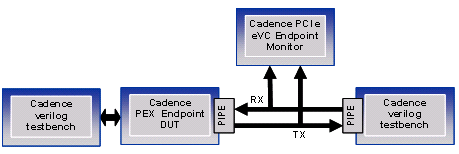
In the verification of our PCI Express Endpoint Controller we made use of both Denali PureSpec VIP and Cadence’s own e Verification Component (eVC) for PCI Express. This was useful both from a verification perspective and in the support of PEX IP users looking to use either VIP solution in subsequent developments.
Here we will focus on describing the use of the eVC as a monitor on the link between the testbench and the PCI Express DUT as shown in the above diagram. The monitor would check for protocol violations on the link and report on any problems. A surprising number of problems were discovered and diagnosed using this setup.
An alternative approach to the transaction based setup shown above uses eVCs to an even greater extent. In this method we come even closer to modelling an entire system. For this approach, two additional eVC agents were added to the verification platform. An eVC which modeled a PCI Express root complex was connected in addition to a second monitor as shown below. The second monitor was used to check the root complex link protocols.
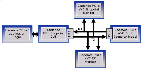
On the left hand side of the diagram it can be seen that there was still a certain amount of logic required to model an application layer for the design. The advantage of using an eVC as a model for the root complex is that eVCs are coverage driven models. The eVC will automatically generate data items, interrupt types, data sequences etc. The root complex eVC is randomly driven initially meaning that over time a massive number of legal and also illegal transactions may be modelled. The level of randomness is controllable however which is helpful when attempting to target specific corner cases. The extent of the ‘soft’ verification performed on the design gave a high level of confidence in the eventual performance. At this stage, prior to moving on to a completely hardware platform such as FPGA prototyping, it is extremely beneficial to be able to emulate on a Palladium.
Prototyping and Hardware Verification
There are a number of benefits evident to using an emulation system such as Palladium rather than simply moving on to prototyping or even silicon.
Long before silicon is available a software team can begin to develop software and drivers for an end product on a synthesised version of the end design running at many times simulation speed.
A design being emulated on a Palladium may be probed in the same way as a simulation, memories may be interrogated and populated via the user interface, signals may be forced, and complicated triggers are possible.
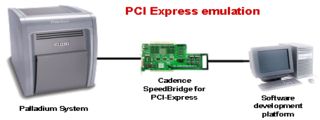
Cadence Design Systems, Inc. has developed a range of SpeedBridge cards, one of which is the PCI Express Forward SpeedBridge. This card is used to bridge between an emulated design running at emulation speed on a Palladium, and a real world application such as the root complex in a PC main board, running at full speed. A debug display is present on the SpeedBridge card which allows the user to examine the number of packets of a specific type which have been transmitted or received. In addition to the display there are a number of status LEDs which can provide rudimentary information such as system heartbeat or link status.
In the layout shown above, the PCI Express endpoint design has been synthesised and uploaded into the Palladium. This endpoint design then communicates via the SpeedBridge card with the mainboard inside the PC. With the system setup in this way it is possible to boot the PC and write or install drivers to control the emulated endpoint device.
The endpoint design interfaced to a small memory which was enough to allow the PC to perform memory reads and writes, proving the functionality of the system.
FPGA Prototype / Protocol Analyser
The final verification stage was to take the design from emulation and port it onto an FPGA prototype card.
The main problem with prototyping in this way is that debugging a design without access to internal signals or by trying to capture traffic over a high speed serial link is incredibly difficult.
The solution found for this was to use a protocol analyser. After investigation into the various options available in this field, the design team settled upon an offering from Catalyst Enterprises Inc. which appeared to offer the best functions.
The Catalyst Protocol Analyser may be used in a number of modes. It comes with its own backplane containing two PCI Express slots and may be used in exerciser mode, where the Catalyst will operate as a root complex and drive the link. It may also be used in analyser mode where it is plugged in between a real mainboard and the endpoint card under test and will capture all of the traffic across the links.
The software suite which is delivered with the Catalyst is extremely configurable and can be set up in various link width configurations and with a multitude of triggers possible. By using the catalyst in these modes it was possible to fully examine all of the traffic over the serial links and to quickly debug any problems. The analyser will report on any protocol errors seen. A further use was to write small test cases using the Catalyst software which were able to read and write to various configuration registers and setup the card in different modes.
Compliance
PCI SGI provide a test suite for PCI Express designs which are used to verify that specific cards or designs are fully compliant with the latest version of the PCI Express specification.
With the design fully verified the card was taken to the PCI SIG Compliance Workshop where it passed, allowing the Cadence PEX to be added to the PCI SIG Integrators List.
Conclusion
In looking at a PCI Express development we have been able to see that there are a wide range of verification tools available to de-risk and accelerate the verification process.
By using a verification methodology which takes advantage of these solutions developers can dramatically reduce the likelihood of re-spins due to functional bugs.
A multi-layered verification methodology which is customised to the requirements of a particular standard is of great benefit when preparing for compliance testing while minimizing development timescales.

