Mana Coste and Emmanuel Riou from Wipro-NewLogic
The issue of integration is driven by both advances in technology and changes to the market space. In many cases the business changes help drive uses of the technical improvements, so we begin by looking at the commercial landscape before examining the technical environment and, in particular, the ongoing debate of CMOS vs SiGe.
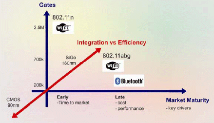
Wireless chipset / SoC design choices are driven by many orthogonal goals and hence the decision space is multidimensional. Picture 1 below attempts to place some current wireless technologies in three of the possible dimensions (complexity / chip(set) size, market maturity, and integration vs power efficiency), however these are far from the only dimensions possible.

Picture 1: The more a product penetrates the market, the higher is the pressure for an efficient integration module
The Wireless/RF market

Picture 2: At the beginning of the life cycle, time-to-market is dominant. For mature products, cost reduction becomes more dominant
Wireless communication is becoming more and more commoditized. While newer technologies such as UWB and 802.11n are still in the early adopter phase, with time to market being the primary driver, the markets for Bluetooth and 802.11abg are maturing, meaning that cost reduction becomes the primary goal. This, in turn, implies greater integration of components and the use of off-the-shelf designs to decrease risk and time to market. Fortuitously, such integration also grows the market by reducing power consumption and simplifying incorporation into consumer devices. Integration is also assisted by the maturity of the CMOS process, which presents numerous advantages for RF as well as digital use at smaller geometries such as 90nm.
Bluetooth, which started as a wire-replacement technology for mobile handsets and headphones, is now evolving into more general purpose streaming audio applications. The digital part of Bluetooth is small (less than 200k gates), so its integration with RF into a single 130nm package is standard. At 90nm it becomes interesting to incorporate both digital and RF as a small part of a larger ASIC.
The earlier 802.11 standards are also mature, with a tendency for different chipsets to be used in different applications. Critically, driven by the arrival of 802.11n, the adoption of 5Ghz radio is becoming more common. As with Bluetooth, there is a desire to reduce the chip count by integrating the entire stack, including the RF as a part of a larger ASIC or SoC. One key reason why 90nm CMOS is of interest in this space is that, unlike earlier geometries, 90nm can easily support the required 5Ghz frequency RF components at a reasonable power consumption. This also makes it easier for 802.11 chipsets to be reduced to a single chip, thus permitting equipment manufacturers to make simple choices between integration strategies.
Little of this is specific to wireless; the same trend of integration from multichip to single chip to ASIC component has been observed in practically every technology.
However, as integration proceeds, the value of off-the-shelf silicon IP becomes ever more important for the following reason: widespread adoption means that manufacturers who are not experts within the field, and need to introduce products that use the technology in as low risk a manner as possible, are able to use designs that have already been deployed in the field.
Migration from chipset to SoC component

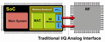
Picture 3: Traditional I/Q Analog Interface

Picture 4: Digital Interface
The migration from the traditional split of digital and RF in two separate packages (picture 3) to a single combined package need not be done in one leap. Simply migrating some digital components and the ADC/DAC to the RF side of the split (thus replacing a traditional I/Q analog interface with a digital one) provides significant benefits. By making the MAC/modem purely digital, it is much easier to integrate that functionality into a larger ASIC (picture 4), which permits faster release of chips using newer smaller geometries and reduces the test load. Because digital signals are less sensitive to line noise etc., this also drastically increases board layout flexibility and permits the analog RF to be optimally positioned adjacent to the antenna. This migration strategy allows a gradual decrease of the relative proportion of the RF area as more and more digital processing (e.g. the entire modem function) is moved to the RF chip and eventually enables an integrated single chip solution.
The integration benefits of CMOS
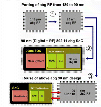
The key to this strategy is the use of CMOS for the RF. Implementing the RF in CMOS as opposed to SiGe provides a lot more flexibility to reuse the layout in different ways. Consider an example roadmap for 802.11 RF from a chip company, and the implications of choosing CMOS for the radio. As picture 5 shows, once the RF is ported from an older technology to 90nm CMOS it can be used both as part of a single ASIC that requires 802.11abg connectivity and as a building block for a separate 2x2 802.11n RF matrix element.

Picture 5: The different steps to a SoC
In the SoC case above, the RF is integrated with a compatible 802.11abg MAC and modem and the combined MAC/modem/RF block is then made available as a standard component that may be used in numerous different SoC applications. Although the package is larger than, say, a Bluetooth equivalent, at around 700k gates and 10mm2, it will still be a comparatively small portion of the final SoC. At such a size it becomes commercially attractive to integrate the complete WLAN functionality into an ASIC, whereas with larger CMOS geometries it would not have been cost effective.
In the 802.11n case the RF layout is duplicated and the two laid out side by side. They two can reuse blocks common to 802.11abg and 802.11n (PLLs, LNA etc.), but other sections such as the ADC and DAC require modification to make them compatible with 802.11n. Such reuse dramatically improves the ROI calculation for the initial porting and also assists the development of 802.11n systems by drastically reducing risk factors.
The risk is reduced two ways. Firstly the original 180nm RF is a proven design that is then ported to 90nm. Although there may be issues with the port (lower voltage, leakage effects, differences in parasitics and so on), because the RF does not need to be designed from scratch it is comparatively straightforward and is known to be compliant with the 802.11 standards. Secondly, once ported, it can be incorporated into any number of chips (including, if desired, a single 802.11abg only chip), and thus its compliance with 802.11 can be confirmed.
The CMOS vs SiGe Debate
One of the big areas of debate is between CMOS and SiGe for analog RF. Traditionally SiGe seems to have been preferred because it is believed to require lower power and be more reliable in terms of design yield – that is to say the risk of requiring a respin is lowered – but CMOS offers many factors that make it more attractive for modern geometries. In particular, although CMOS at 90nm may require a higher current than SiGe at 180nm, the overall power consumption is typically similar because the supply voltage is 1.2v instead of 1.8v.
The key to using CMOS for RF is that, as mentioned earlier, 90nm CMOS is mature, with a full range of PDK’s, libraries, tools etc., and at 90nm is able to support the 5Ghz frequency bands. Thus even if a SiGe design is more power efficient for a particular RF application, SiGe blocks integration onto a single chip. When the RF is integrated into the SoC with the rest, the fact that it is on the same chip allows up to 50mw of power saving through the elimination of intercommunication over the PCB. As well as reducing power consumption, this integration also reduces cost (fewer pins) and PCB size (one chip not two), thereby significantly reducing the overall manufacturing cost.
On the other hand, a combined application plus baseband plus RF chip is itself significantly more complex than any part of a chipset that provides the same result, so while board layout is simplified this comes at the expense of significantly increased chip complexity. The risk of failure can be reduced using standardized components, but even so the combination presents some technical challenges. One critical issue is that RF typically requires 6 layers, whereas the digital part may need up to 9. The extra layers are required for digital to obtain an optimum die area, whereas in many case for RF the use of the extra layers adds no value (a certain amount of space between blocks is often needed in order to avoid noise injection through coupling). A second, somewhat related, issue is that of leakage: particularly in the case of applications where significant sleep time is anticipated, leakage effects in inactive components can cause significant wastage. Careful design using power islands or other more elaborate techniques can reduce this by between 40% and
80%, but this may well lengthen the design cycle and impact time to market. Finally, the coexistence of digital and RF components may result in noise from the substrate and power supply. Again, there are design tricks to minimise this: careful floorplanning of building blocks, particular attention in the choice of an optimal substrate for noise isolation and a high number of power supply ESD domains all help to resolve this issue.
In addition to the integration benefits that typically apply, in contrast to SiGe, the use of 90nm CMOS for RF provides a number of key advantages over older, larger CMOS geometries. The ability to handle higher frequencies (over 5Ghz) is, of course, critical. This comes from faster switching and lower power requirements for LNAs, pre-PA mixers and VCO/Synthesizers, as well as the ability to use PMOS for RF. This latter is a result of the reduction in component size, and hence signal distances, which therefore means that the inherently lower mobility of the PMOS is no longer an issue. Another benefit is the smaller size of the entire layout. Passive components can be far more densely laid out, and capacitors, for example, are typically half the size of 130nm ones.
Conclusion
Full SoC integration is clearly not suitable in all environments. For early markets the transceiver will remain a chipset; however, the pressure to integrate increases as the technology matures. In the SiGe/CMOS area there are two distinct options. One is the dual SiGe/CMOS solution, with its relatively clean demarcation point and its ability to use both low current SiGe and the smallest, lowest powered CMOS geometry. The other is the fully integrated CMOS approach, which permits single chip solutions that have equivalent power savings and reduce overall device cost. As the leading wireless IP vendor, Wipro-NewLogic are able to base their analysis of industry trends on years of relevant experience within the industry and a unique understanding of CMOS RF strengths and weaknesses. It is critical to consider the entire product / technology life cycle when starting a new program and selecting an RF technology. Expertise in software from device driver to the application layer – as well as in RTL, signal processing and RF – is critical to ensure the correct level of integration as the market matures. It is clear that CMOS is not the universal winner: nevertheless, as WLAN technologies mature, the commercial advantages of integration presented by CMOS will tend to overshadow the technical advantages of SiGe. In fact, when looked at from the perspective of an entire system, frequently the CMOS approach will also win from a technical perspective, because the integration allows for total device efficiencies that more than make up for individual subcomponents that are not as good as their SiGe alternatives.
Contact:
Millennium Park 6
6890 Lustenau / Austria
Phone: +43 5577 995-0
wnl-contact@wipro.com
www.wipro-newlogic.com
