By Fuad Abu Nofal & Monica R. Nofal,
ChipEDA
San Jose, CA, USA
Abstract
As the number of transistors doubles almost every two years, the ability to use a flat approach for full chip floorplanning and perform flat P&R is hindered by the capacity limitation of current EDA tools - even though the EDA tools have expanded their capacity. In this paper we will show a top down hierarchical chip floorplaning methodology for a large SoC allowing the reuse of blocks in the same chip, as well as in different chips. We will show how the same hierarchical approach is applicable to smaller chips accelerating design closure.
Using a “divide and conquer” approach, the design is partitioned into smaller physical blocks and the means to manage the complex process of hierarchical design flow is provided. This important combination enables designers to ReUse these physical blocks resulting in shorter design cycles.
1. Overview
We will cover the method used to partition the design into smaller blocks and show how we generated consistent design views:
- block timing constraints (tcl- SDC format)
- block timing abstracts (LIB timing model)
- block physical constraints (DEF – fplan with shape, area, pins, PG grid)
- block physical abstracts (LEF – with shape, area and pins)
In addition, the top level floorplan was generated with the details of all the hierarchical blocks included:
- placement of all top level pins
- placement of all hierarchical blocks, with their pin assignment
- top level PG
This allows the design team to progress on the block level as well as on the top level simultaneously.
We will show how we solved the problem of routing global signals over the blocks while preventing the possibility of cross talk between the top level signals and the hierarchical blocks. In addition we will show how we generated accurate timing budgets for each of the hierarchical blocks while taking into account the top level wire delays.
We will show how we used Chipmason, an EDA tool from ChipEDA, in combination with other tools to perform the above flow.
2. Design Example
We will use a simplified SoC example to demonstrate the design methodology described in this paper. The SoC consists of an embedded CPU (sdu) with its instruction and data cache (idu, cbu), a media processing unit (mpu) and a media acceleration unit (mau). It includes three small units to support status, control and clocks (stu, bcu, cku).
The SoC has 8 identical external peripheral interfaces (pru blocks) and a data cross bar which transfers data to/from the main memory interface and the main processing units as well as the external interface units.
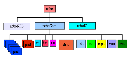
We will focus on the core floorplan (neboCore) of the chip, and will not discuss io ring related issues.
2.1. Design Partitioning
In order to get the biggest benefit from the top-down hierarchical approach, the design team should start working on the floorplan as early as it has the chip top level interconnect. In fact the floorplan at this time is just a simple drawing showing the physical block diagram, where the area can be estimated.
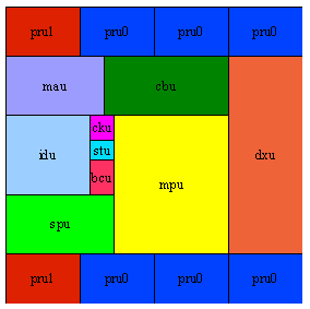
Initially the physical design hierarchy can follow the logical design hierarchy as can be seen in Figure 2. Later in the design phase, big blocks can be split into smaller ones or small blocks can be combined into one physical block. Chipmason has powerful netlisting capabilities, which can quickly repartition a design and make it “physical design” ready.
2.2. Design Flow
The design flow described below was used to design several SoCs. Most steps of the flow are based on the Chipmason™ tool set, except for the logic synthesis, the final Place and Route and the final timing signoff. This flow was integrated with tools from other vendors: the Synopsys tool set, where we used DesignCompiler for synthesis, ASTRO for P&R and PrimeTime for timing verification, and the Cadence tools, First Encounter and NanoRoute.
2.2.1. Synthesis phase
The main focus of this phase is to create budgets for synthesis and refine the floorplan:
- Start from RTL netlist to get the basic connectivity of the top level blocks
- Initial floorplaning: Area can be based on estimates (or can be accurate if any of the blocks is an IP)
- Initial timing budgets are based on user inputs, and on the initial floorplan. The timing for all the top level wires is calculated and budgets are allocated to the different blocks. This process will take into account the wire delays of all top level signals (based on placement of blocks in the floorplan)
- The resulting timing budgets are fed into the synthesis flow. Netlist generated after the synthesis will include the effects of top level routing and buffering.
- Upon completion of the synthesis, the resulting netlist will be verified, performing timing analysis. Block sizes will be adjusted
- The hierarchical floorplan will be adjusted after every new synthesis release and new timing budgets generated
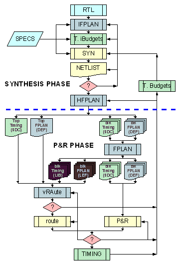
The quality of the results is expected to improve after each iteration. While the RTL will be stabilized for some blocks and still changing for others, the feedback time budgeting process (T. Budgets) will be repeated for every new netlist release and new time budgets will be provided for each block.
2.2.2. P&R (Place & Route) phase
This phase starts with a more accurate floorplaning, optimizing block pin placement, and planning the details of the global clock distribution
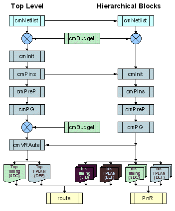
- The refined hierarchical floorplan (HFPLAN) will generate a consistent set of design constraints and abstracts.
- Each physical block will have matching timing constraints and timing abstract, as well as matching physical constraints and physical abstract.
- The timing and physical abstracts of each hierarchical block are used for the top level floorplan and later for the final place and route task.
- The timing and physical constraints of each hierarchical block is used to perform additional floorplanning iterations at block level. At this time the shape of the block, its pins, its power grid are fixed and cannot change without impacting the top level floorplan.
- The revised block level floorplan will entail macro placement optimizations, pre-placement of critical logic, isolation buffer insertion, repeater insertion. The most important outcome of this new floorplan is repeater insertion in the block that will be used by the global route. In addition routing channels are reserved in the block itself to allow over the block routing. Details about this process are given in section 3.3.
- After the detail floorplan is generated, the block is placed and routed. The timing is verified against the constraints.
- Before the final place and route for the top level, a new set of block physical abstracts are used (which were generated during the detailed block floorplan and which include repeaters inserted in the block as well as routing channels in the block)
- A repeater allocation and global routing program (vRAute part of Chipmason) is run. It analyzes the top level floorplan and connectivity and the timing constraints and checks for resource availability (checks for top level repeaters in the block as well as routing channels resources). The program performs timing and congestion driven global routing. It generates a new top level netlist with the repeaters allocated to the global wires.
- The new floorplan and netlist are sent to the final step of this phase; top level place and route.
3. Design Flow Details
In this section we will cover the details of this design flow. We will show which parts of the flow use our tool and which parts can use any available commercial tool. This flow was successfully used in conjunction with the Cadence, “Encounter” tool set and with the Synopsys DesignCompiler and Astro tool sets.
3.1. Time Budgeting
It is essential to create accurate timing constraints and abstracts when using a hierarchical design approach, but achieving this goal requires several iterations. It is not practical to wait for the details of each one of the hierarchical blocks to be able to create timing abstracts, nor is it efficient to ask the designers to create specs for their block. Top level interconnect delays are a dominant factor in the over all system speed, making it mandatory to take top level interconnect into account when budgeting the time for each one of the blocks.
In addition, any block placement change in the top level floorplan, or change in block shape and/or pin assignment will affect the top level wire delays and will change the time budget allocated to the blocks themselves. We used “Chipmason” to integrate the time budgeting with the floorplanning task, regenerating a new set of timing budgets every time we modified the floorplan and each time a new chip netlist became available. During the early stages of the floorplanning task, top level routes are estimated, and wire delays are calculated.
When the design is complete, we read the full chip netlist, using Chipmason’s internal STA, to find the critical path through each pin of each instance of the top level. These paths set the timing constraints for each one of the blocks and the constraints for the top level. The delays inside the block and the top level wire delays are taken into account in this calculation. The outcome of this phase is a new set of timing constraints for each of the blocks and a new set of abstracts to be used in the top level P&R.
Two special cases should be taken into account. Some blocks may have been designed earlier and their timing constraints and abstracts cannot change. In this case the block is given the “frozen” property and the time budgeting will involve only the blocks in the design process. This is important, because many SoC designs use hard macro IPs. The second case involves multiple instantiations of the same block. The top level wire delays may be different for each instantiation. In order to use the same physical block in a variety of contexts, Chipmason will perform worse case timing analysis to ensure that no matter how the block is used, it will have timing budgets that meet the final spec of the SoC.
3.2. Hierarchical Blocks Shape, Area and pin assignment
Chipmason is a complete floorplanning and silicon proto typing tool. It can be used to perform the detailed floorplan for each one of the physical blocks in the design. It creates the exact shape of
3.3. Buffer Insertion at the block level
An initial block floorplan is generated at the HFPLAN stage, where the shape of the block and its functional pins are allocated. This floorplan is read into the second, detailed floorplaning stage of each block, where the full netlist is read, and macro blocks are placed. The users add additional features to the floorplan, and repeater stations in the block.
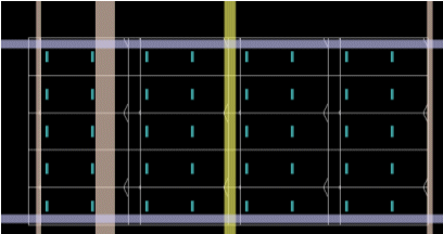
Each repeater station is shielded from the surrounding logic and routing by adding power wires around each station.
To improve the routability and to optimize the utilization of the repeater resources, repeater stations come in two different types, horizontal repeater stations which are optimized to buffer horizontal wires and vertical repeater stations which are optimized to buffer vertical repeaters. During the allocation process, repeaters can be used for either direction.
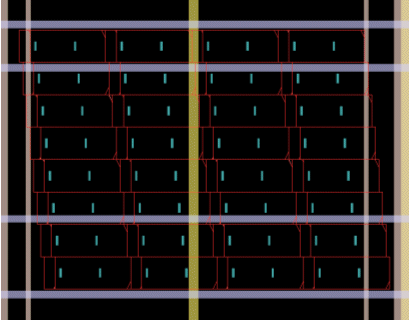
New pins are added to the block to allow the top level to utilize the repeaters inserted in the block. The repeater pins can be allocated using higher metals to ease their connection when used at the top level.
Routing channels will be reserved over the repeater stations to allow the top level to route over the block. The block floorplan will have placement obstruction were the repeaters are inserted, and will have routing obstruction over the repeater routing channels (in the metal layer specified for the top level routing)
Different types of repeaters can be inserted in the block: small buffers, large buffers or clock buffers. If different types of repeaters are inserted, a repeater property is added to each one of the pins to enable the top level to optimize the repeater allocation.
3.4. Virtual routing while performing Repeater Allocation – vRAute™
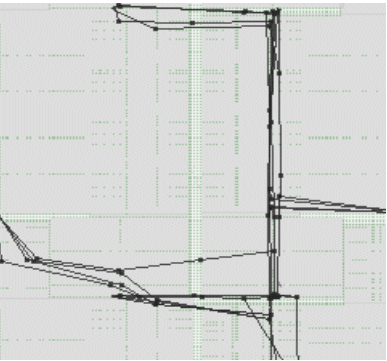
During this stage, the new hierarchical blocks’ abstracts are read into the top level HFPLAN - these abstracts include new repeater pins (with repeater type property) – and then Chipmason-vRAute™ is run. It will perform very fast global routing while allocating the repeaters from the blocks. The tool has an option to allow it to insert additional repeaters in the routing channels if such channels are available and free. vRAute will take into account the timing constraints as well as the availability of resources. These resources include the availability of repeater buffers and routing channels.
4. Physical block ReUse
The hierarchical design approach has been used for many years. It has allowed design teams to partition their design into small blocks that could be handled by the available EDA tools. The users of such an approach had two different methods when it was time to do the top level routing:
- Either they had to route over the blocks importing the top level wire into the block P&R. This approach is sometimes called the “abutment approach”. The draw back of such an approach is that any change to the top level will impact the block level and any change to the block pinout affects neighboring blocks and the top level. Furthermore, the top level wire embedded in the block level will suffer from cross talk with the block wires, and the timing closure will suffer.
- Or they had to allocate routing channels around the hierarchical blocks to allow routing of top level signals in these channels. This approach solves the problem on interaction between the top level and block level, but it is extremely ineffecient. The top level wire can be 2-3 times longer than the shortest path possible.
The design flow described above, using Chipmason™ EDA tool, allows routing over the block using pre-allocated routing channels and benefiting from the repeater already inserted in the lower level blocks. In addition, by shielding the routing channels from the block level wires, we ensure that the block level timing can be closed independently of the progress of the top level and vice versa. This last feature will allow the re-use of the block multiple times in the same chip or in different chips.
5. Conclusions and Recommendations
Using a hierarchical design approach allows the design team to divide the chip into manageable blocks, and reduces the time to results while improving the quality. The flow discussed above, based on Chipmason, allows complete integration of all aspects of hierarchical design, floorplanning, time budgeting and buffer insertion and allocation while enabling reuse.
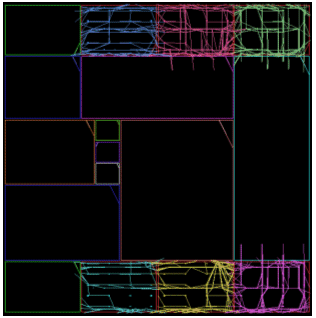
Most important about the reuse methodology is that each block is designed independently of the top level. Furthermore, the top level place and route task is independent of the hierarchical block as it relies only on the block abstracts. The routing over the block will not impact the hierarchical blocks’ timing – block repeaters and routing channels are shielded from intra block wires – which allows the design team to work simultaneously on top level and block level.
6. Acknowledgements
We would like to thank our colleauges Alec Panoviciu, Ionut Cirjan and Marius Piper who helped design and integrate the flow. Also, we would like to thank our customers for their valuable feed back which allowed us to enhance the tool and the flow.
7. References
There are numerous references to the advantages and benefits of a hierarchical design approach.
I. Chipmason manual: www.chipeda.com
II. “Buffer allocation algorithm with consideration of routing congestion” – by Yuchun Ma et al
III. “Integrated Floorplanning and Interconnect Planning”– by Hung-Ming Chen et al.
IV. “A practical methodology for early buffer and wire resource allocation” – by Charles Alpert et al
V. “Simultanous floorplan and buffer-block optimization”– by I. Hui-Ru Jiang et al
