Wipro Technologies, Bangalore, India
Abstract :
The shrinking process geometries are enabling to build more complex SoCs, which has higher risk of re-spins. The FPGA prototyping is an efficient approach to perform pre-silicon SoC validation, accelerate system software development and to meet time-to-market demands. The first few major steps in FPGA prototype development are SoC RTL migration to FPGA(s) and design-for-debug, which are predominantly manual processes. For FPGA prototyping exercise to be successful; it is very important to meet criteria such as short development/turn-around cycle, code maintenance and ease of debug. In this paper, RTL migration and debug strategies are presented, which needs to be skillfully handled to meet the said criteria. This paper is backed up with vast FPGA prototyping experience of various SoCs with logic gate count up-to four million.
1. Introduction
The exciting benefits of FPGA prototyping are ability to fine-tune hardware/software portioning, integrated hardware/software testing and validation in end-application deployment scenario.
Following are the objectives for FPGA prototype to be effective:
a) Quick and fool-proof migration of SoC RTL to FPGA(s), with minimal change in control structure (clock and resets) and without affecting the target functionality.
b) Easier SoC and FPGA prototype database maintainability
c) Design for ease of debug
d) Minimal and clearly identified changes in the Firmware which is running on FPGA prototype platform to run on SoC post-silicon validation platform
e) Shorter turn-around cycle from SoC RTL bug fixes and enhancements to FPGA bitmap generation with consistent results
f) Optimal type/number of FPGA(s)
g) Higher system performance
The said objectives can be mainly grouped into following five categories:
a) SoC RTL migration to FPGA(s)
b) Selection of off-the-shelf FPGA prototype platform or FPGA device selection incase of custom-built platform
c) Design-for-Debug
d) FPGA Partitioning and
e) Timing closure
In this paper first three categories are covered (a, b and c), where as FPGA Partitioning and Timing closure categories (d and e) are covered in author’s another paper [1].
Following are major challenges in achieving said objectives:
a) Change in target library: SoC code is targeted for Foundry specific library and might be using specialized components/IPs. Mapping of this SoC RTL to chosen FPGA(s) by maintaining functional equivalence is crucial
b) RTL code sync-up and database management: Maintainability of SoC and FPGA prototype databases and sync-up for bug fixes and enhancements
c) Design-for-debug: FPGA prototype system should ease intra and inter-FPGA debug and problem isolation
d) Minimal Firmware changes: The amount of changes needed in the Firmware which is running on FPGA prototype should be minimal and clearly identified to run on SoC post-silicon validation platform
The said challenges have to be skillfully handled to meet the FPGA prototype objectives. This paper presents in-detail the said challenges along with efficient methods to tackle them. The section 2 highlights prerequisites of FPGA prototyping. The section 3 describes in-detail RTL code migration and prototype platform/FPGA selection procedure. The design-for-debug aspects are covered in section 4, followed by conclusions in section 5.
2. Prerequisites of FPGA prototyping
FPGA validation engineers have to work closely with SoC designers and Firmware engineers to build an effective FPGA prototype platform. Apart from the knowledge of high level SoC architecture and limited knowledge of micro-architecture, FPGA validation team has to capture vital information as given in Table 1, from SoC designers:
| S.No | S o C Design Attributes |
| 1 | Combinational Gate Area (2-input NAND gates) and Number of Flip-Flops |
| 2 | Number of clock domains, frequency targets and gated clocks information. Also information of derived signals being used as clocks if any. |
| 3 | Clock controller details such as PLLs/DLLs, Clock Multiplexers and Dividers |
| 4 | User IOs with special requirements such as SSTLII and LVDS |
| 5 | Number of Resets (Synchronous or Asynchronous) |
| 6 | Maximum number of 2-input NAND logic levels between – Register to Register; Input to Register; Register to Output |
| 7 | List of Memories/Register Arrays used – Type, numbers, size and access latency |
| 8 | Special SoC foundry library specific macros, IPs used if any |
| 9 | Details of the Embedded processor and internal bus structure if any |
| 10 | Any exceptions allowed in FPGA validation such as combining different clocks and resets |
| 11 | Concurrency requirements of SoC logic to be validated. This will help in minimizing number of FPGAs needed with multiple bitmaps of varying functionality. |
| 12 | The list of desired debug signals |
Table 1 SoC Design Attributes
Based on the FPGA mapping process, there might be few minor changes in the functionality (e.g. SW configured soft-resets may be combined with system reset in FPGA validation due to simplicity), which needs to be communicated to Firmware engineers.
3. Prototype platform/FPGA selection and RTL code migration
3.1 Prototype platform/FPGA selection
The SoC design attributes gathered (as per Table 1) can be used as guidelines for choosing off-the-shelf FPGA prototype platform or selecting the FPGA(s) if prototype platform is being custom-built. The main criterion for such selection is gate count, memories, PLLs/DLLs, clocks/resets, embedded processor, number of IOs and IO standards. The chosen FPGA resources should be at least 30-40% higher as RTL might not have been matured at the start of prototype development cycle.
3.2 RTL Code Migration Aspects
Migration from SoC to FPGA requires RTL code changes, due to various aspects mentioned in this section. Maintainability of the FPGA RTL is one of the critical tasks, as there can be multiple releases of the SoC RTL, while FPGA validation is ongoing. It is not preferred to maintain two different databases and make all the changes manually in the FPGA RTL every time a change happens in SoC RTL. The best approach is to have a single RTL code database for SoC as well as FPGA. The compiler directives can be used in the RTL and conditionally compile code for SoC or FPGA implementations. For example `ifdef in Verilog as shown below for an instance of a buffer (BUFX4) from a standard cell library in SoC RTL:
In this approach RTL code will be the same with code fragments which require modification from SoC to FPGA, enclosed in compiler directives, resulting in far less possibility of functionality mismatch. These compiler directives are to be added in SoC RTL code only once in the beginning for FPGA prototyping. After these changes are made in the RTL code, it is preferred to run basic RTL simulations for SoC as well as FPGA implementations.
Aspect-1: Availability of IP’s in various forms
Various IPs such as DesignWare used in SoC might be available in RTL or technology independent Netlist (e.g. GTECH) form. If IP is available in RTL form, then it can be directly synthesized by the synthesis tool. On the other hand, if GTECH netlist is available, then GTECH components are required for synthesis. Some of the synthesis EDA tools available may or may not support DesignWare IP’s for FPGA synthesis.
Approaches:
In case IP is available in Synopsys .db netlist form, Synopsys synthesis tool (FPGA compiler) is required; else IP can be requested to be made available in GTECH netlist form. The GTECH netlist can be synthesized with Synplicity tools as these tools have Verilog GTECH library. There are synthesis tools (e.g. Certify from Synplicity Inc.) which supports synthesis of DesignWare components, but all components may not be supported. In such scenario, DesignWare components functional description needs to be either created in Verilog or a GTECH netlist shall be made available for the component.
Aspect-2: Memories & Register Arrays
Almost all SoC designs usually comprises of memories in various configurations such as single port, two-port, true dual-port or register files. As the technology is advancing and feature size is shrinking, more logic can be accommodated in the same silicon area, resulting in large number of memories with different sizes and configuration being part of the design. As all the SoC memories are instantiated as hard-macros, only simulation models are available and require generation of FPGA specific memories for implementation in FPGA.
Approaches:
One approach is to create memory wrappers (Figure 1) with module and port names same as that of SoC memories, which instantiate memories generated using the FPGA vendor specific tools (e.g. Coregen from Xilinx and MegaWizard Plug- In Manager from Altera). This approach will not demand any SoC RTL changes by keeping the port names same.
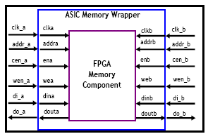
Figure 1 SoC memory wrapper
Second approach is to develop a script, which can generate FPGA memory implementations using the SoC memory nomenclature with FPGA components (e.g. BRAM or SRL16 in Xilinx). This would be possible if SoC memory nomenclature contains the information about the type and size (e.g. ram_2p_4b_128x32 is a RAM name, where 2p specifies a dual-port ram, 4b specifies number of write enables, 128 depth of the RAM and 32 width of the RAM). If memory nomenclature is not maintained in SoC RTL, a spreadsheet saved in text format (comma delimited or tab delimited) containing memory information (as split above) can be input to such a script. Although this approach looks complex, it is a long term solution as this script would work for all designs as long as FPGAs from the same vendor are being targeted. Register files can be implemented using single-port or dual-port memories in FPGA. These components provide area advantage in SoC implementation. But in case of FPGA implementation, it would be preferable to implement register files using RAM (e.g. BRAM/SRL16 in Xilinx flow or M512 in Altera flow) components. This avoids unnecessary routing congestion.
Aspect-3: Other Hard- Macros
Hard-macros are blocks which are directly merged in the physical design stage of a SoC implementation and only simulation models are available for functional verification. As there is no RTL code or netlist available for such blocks, they can not be implemented in FPGA.
Approaches:
If the hard-macro is driven from digital portion of the SoC, i.e. if the macro is used as translation interface between digital logic and pads, it can be removed completely or the connections to the macro can be brought out on ports, limited by the number of IOs available. For example a DAC which is used to drive an analog output corresponding to the value provided by the digital logic can be removed. If required, DAC functionality can be achieved with on-board discrete DAC chip.
But if the macro drives digital portion of the SoC, then its functionality is a must for FPGA prototyping. In this case also all the connections to the macro shall be brought out on ports at toplevel. For example functionality of a frequency synthesizer can be achieved using an on-board PLL and driving the macro ports brought at top level. This might not provide the complete functionality of the SoC macro, but will enable verification of most of the functionality. For example, if an onchip frequency synthesizer provides clock switching by programming control registers, such functionality may or may not be possible to be implemented using discrete PLL chip. The migration of SoC RTL to FPGA will be tedious, if the hard-macros are instantiated deep in SoC logical hierarchy.
Aspect-4: Buffers used for delay
Often SoC RTL might have instances of library components such as buffers to implement delays. For example data strobe signals (DQS) in DDR memory interface needs to be delayed for proper sampling of read data. These delay buffers are not available in FPGA and hence not synthesizable.
Approaches:
The FPGA implementation does not provide the liberty of using buffers for delay. Any such functionality needs to be implemented with alternative ways. For example, as the FPGA prototype platform is expected to run at not very high frequency, the read data from DDR can be sampled with 90-degree phase-shifted clock by ignoring DQS. However if the FPGA family has special components for DDR interface implementation, then they can directly be used. For example Virtex-4 and Stratix-II has IO delay modules to provide delay to the desired signal. Also Virtex-4 IO delay module provides the capability of runtime fine-tuning of delays which will help in realizing instrumentation circuitry for DQS. The above said strategy is to be implemented such that there are minimal changes in the memory controller, preferably only the data transmit and data sample block shall be modified. And functional equivalence with SoC RTL can be confirmed by simulation sanity check.
Aspect-5: Clocks with gating
In SoC implementations, clock gating is a common practice to conserve power when a block is not in use. FPGA has limited clock resources (low skew clock lines) with fixed routing. If clock is gated in FPGA implementation, it departs the clock plane and will be routed using the normal route, which leads to excessive skew and delay compared to clock plane.
Also occasionally derived signals are also used as clocks in SoC implementations. But in FPGA designs, it is not possible to route such derived signals as clocks with low delay and skew.
Approaches:
The issue of clock gating can be handled by the synthesis tool (e.g. Certify) by translating them as clock enables. However there are limitations in implementation of a XOR gated clock with such tools. One method to implement XOR gated clock is using BUGMUX (Global clock buffer multiplexer) available with Xilinx devices as shown in Figure 2. The CLK_180 is 180-degree phase-shifted CLK, which can be generated with on-chip DLL/PLL.
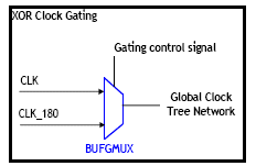
Figure 2 XOR Clock gating
Also if very few flip-flops are clocked by derived signal, it is recommended to re-code that part by using derived signal as clock enables.
Aspect-6: Test/DfT and MBIST logic
Test/DfT logic is an integral part of any SoC implementation. It is usually not required in FPGA prototyping, as this is not the target functionality to be verified. Also if present, it will add extra logic and results in unnecessary routing congestion and timing closure issues.
Approaches:
Test mode enable pin can be tied to disabled state resulting in removal of test logic by the FPGA synthesis tool.
Aspect-7: Clock muxes, PLLs, Buffers
Usually SoCs have got multiple clock domains, which are generated by clock controller module. The clock resources available are limited in FPGA. Also in SoC, some modules might boot up at a lower frequency and later the frequency might be increased for better throughput. In such cases options are limited in an FPGA implementation. For example if PLL/DLL is used for clock generation, the output clock from PLL/DLL can not be controlled further in FPGA as the clock multiplication factor is fixed for a given bitmap. Another limitation is the number of clock multiplexers available in the FPGA. Also usually the clock controller in SoC will have hard-macros/buffers instantiated to generate desired clocks under register programming control. This functionality can not be implemented in FPGA.
Approaches:
It is possible to implement limited clock multiplexing in FPGA as the dedicated clock multiplexers are very few. The clock multiplexing can also be implemented in FPGA by introducing logic for glitch-free multiplexer. One approach of implementing clock dividers and multiplexers in the FPGA is to bring-out derived clocks and reenter FPGA from global clock pins (as shown in Figure 3) for effective implementation, ease of timing analysis and reduced run-times.
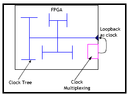
Figure 3 Clock dividers/multiplexers
If the targeted FPGA family supports regional clock buffers (e.g. Virtex-4 or Stratix-II), then clocks need not be driven out and can be connected to regional buffers. However regional buffers should be used judiciously as they are limited and have quadrant based routing limitations. PLL/DLL’s needs to be treated as hard-macros if there is on-the-fly programming involved. And if they are used for de-skewing (phase shift), DLL/PLL available in the FPGA can also be considered. All the buffers need to be removed and equivalent assignment statements have to be implemented in RTL.
Aspect-8: Multipliers
In SoC RTL, multipliers are either instantiated from DesignWare library or left to synthesis tool to infer from behavioral description. Hence these multipliers are not synthesizable for FPGA unless the RTL is modified.
Approaches:
Nowadays most of the FPGA families have multiplier hard-macro elements optimized for performance. The SoC multipliers can be replaced by creating a wrapper for the multiplier core of desired configuration generated by the FPGA core generator.
Aspect-9: Resets
In SoC design, reset generation logic is responsible for generating reset signals synchronized to various clock domains. If all clock domain synchronized resets are used in FPGA prototype, it will cause routing congestion and scenario will be worse if the resource utilization is high.
Approaches:
FPGA architectures are not designed to support complex reset topologies. It is recommended that reset structure for FPGA validation is simplified to a single or reduced number of resets, which can be routed using the dedicated routing resources in FPGA, there-by avoiding congestion. Also it is highly desirable to ignore module level soft-resets and use only global reset.
Aspect-10: IO cells including DDR cells
SoC RTL will have IO pad cells instantiations from standard cell library, hence can not be directly mapped on FPGA.
Approaches:
Migration to FPGA requires replacement of SoC IO pad cells with that of FPGA. One method is to create an IO module, which instantiates FPGA equivalent IO cells. Another method is to replace SoC IO cells with equivalent synthesizable logical assignments (e.g. bidirectional IO cell can be implemented using a tri-state assign statement) and leave it to the synthesis tool to infer the pads. Any special IO cells in the SoC, such as DDR, PCI, LVDS needs special attention. If RTL migration is performed by instantiating equivalent IO cells from FPGA library, then requirements of a particular IO standard are taken care by the implementation tool. On the other hand if the RTL is migrated using logically equivalent assignments, the implementation tool must be provided with information about specific standard IO to be inferred. The above said task can be accomplished with the help of constraints file (e.g. in Xilinx flow IO_STANDARD constraint can be used).
4. Design-for-Debug
Technique-1: Internal Logic Analyzer (LA) design with multiple debug signals multiplexed
The debug logic can be added which acts as chip level Logic Analyzer, i.e. the signals inside FPGA can be monitored with the help of JTAG without bringing out on FPGA pins. Some of the examples are Chipscope from Xilinx and Signal Tap from Altera. The above said technique uses internal RAM blocks of the FPGA to store the samples. Hence there is a limitation on the number of signals and samples which can be tapped. One possible approach is to multiplex signals and control the output to be observed either by using SW configurable registers or by using a virtual IO in case of Xilinx Chipscope.
Technique-2: Adding debug registers
Additional registers can be added for debug purposes, which can be used to monitor signals after a major operation (e.g. DMA transfer or state of a state machine). This is more of a design effort than just a debug strategy. And it has to be incorporated in the design from the very beginning, as it is possible that FPGA prototyping team is not familiar with the design completely and will not able to use this technique efficiently. This approach is even useful for SoC post-silicon debug.
Technique-3: DDR MBIST
It is good practice to verify stand-alone DDR controller RTL in FPGA platform. This is due to the fact that major modifications will usually be carried out to match SoC functionality in FPGA. One best way of doing this is by using memory BIST logic, i.e. the memory controller RTL with a wrapper to control and initiate transactions on the DDR interface (Figure 4). This will help in confirming the sanity of DDR interface before embarking on entire design debug. This will also help in isolating bugs with such a crucial interface in the design. This technique can even be applied to other interface modules, where major SoC RTL modifications have been carried-out for FPGA prototyping.
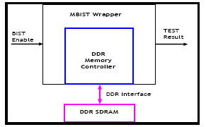
Figure 4 DDR MBIST
Technique-4: IO toggle test
If the SoC prototyping is being carried out on a custom built muti-FPGA platform, IO toggle test can be extremely useful. This test ensures that there are no shorts or opens on the board for signals between different FPGAs. This can also be used to validate whether inter-FPGA timings are met by transferring and capturing the pulses between FPGAs at-speed. Although this test can not help in testing interface to other peripheral components on-board, still majority of the FPGA pins are covered by this test.
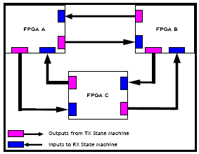
Figure 5 IO toggle test
This test (Figure 5) implementation will be having synchronous state machines in all the FPGAs. All the FPGA interconnect pins are classified as either inputs or outputs based on actual design. Input pins on a particular FPGA are connected to receive logic whereas output pins are driven by transmit logic. Transmit logic generates a walking ‘0’ and walking ‘1’ pattern which is captured by the receive logic in the other FPGA.
5. Conclusions
This paper describes aspects of RTL migration for prototyping SoC on FPGA platform and efficient approaches to handle them. The aspects covered range from RTL database management to replacement of standard cell instances, memories, multipliers, clocks, resets and hard-macros. Also few debugging techniques have been described which will help in reducing the prototype debug time. The said techniques will help in achieving first-time-right apart from shortening FPGA prototype development and debug time.
6. References
[1] Vijay Kumar Kodavalla and Nitin Raverkar, “FPGA prototyping of complex SoCs: Partitioning and Timing Closure Challenges with Solutions”, IPSOC 2005.
[2] William Wu, Dr. Jim Tobias and Bob Uvacek, “Experiences with Multi-Core SoC Designs with FPGA Prototyping”, IEEE HPCA-11: Workshop on Architecture Research using FPGA Platforms, Feb. 2005.
[3] King Ou, “Using ASIC Prototyping to Reduce Risks”, SNUG, San Jose 2005.
[4] H. Krupnova, “Mapping Multi-Million Gate SoCs on FPGAs: Industrial Methodology and Experience”, Proc. DATE 2004.
