Munich, Germany
Abstract:
FlexRay is an upcoming networking standard being established to raise the data rate, reliability, and safety of the automotive applications of today and tomorrow. Synthesizable FlexRay intellectual property (IP) is now available for those who want to integrate it into a new chip. This paper discusses what the FlexRay IP is and how to implement it; highlighting issues, considerations, and solutions for the system designer.
Introduction
Automotive bus requirements for data throughput, fault tolerance, and deterministic behavior have changed dramatically in the last few years. New applications such as stability control and throttle-by-wire require many more electronic components, each screaming for more data, deterministic behavior, and reliability. The FlexRay communication protocol was developed to fulfill these needs.
FlexRay technology can be split into three to main areas: 1) software to configure and manage communication in a FlexRay cluster, 2) digital logic implementing the FlexRay protocol, and 3) analog signal drivers. This paper focuses on the digital hardware elements of the FlexRay IP and considerations when integrating it into an SOC.
FlexRay Conceptual Hierarchy
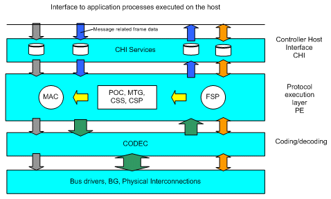
As shown in Figure 1, the central layer of the FlexRay hierarchy is the protocol execution layer, where outgoing frame data is sent to the physical layer. On one side, the protocol execution layer interfaces to a controller host interface, which contains storage for all interface data and provides the controller host interface services.
On the other side, the protocol execution layer interfaces to the coding/decoding layer. The physical layer contains the bus drivers, the optional bus guardians, and the physical interconnections.
Figure 1: Conceptual hierarchy of FlexRay system layers
Conceptual Partitioning
In the design of a FlexRay core, the team should focus on communication-related fault tolerance, not on application related issues such as message agreement algorithms. This paradigm ensures that the design is suitable for different applications with diverse fault-tolerance needs.
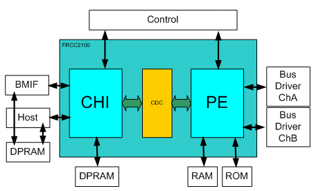
Figure 2 shows an example FlexRay core partitioning in which the Protocol Engine (PE) is responsible for all the FlexRay specific protocol handling and the Controller Host Interface (CHI) handles all the tasks of integrating the FlexRay functionality into the rest of the system.

Figure 2: FlexRay block structure
The CHI provides host access to the FlexRay core’s configuration, control, and status registers as well as to the message buffer configuration, control, and status registers. The message buffers hold the FlexRay frames (received frames and frames to be transmitted), including the frame header and payload data, and frame status information. The message buffer data is stored in the FlexRay memory, while the message buffer control structures are implemented in the CHI.
Different end user applications have a wide range of requirements. Therefore, the core should be configurable so that the integrator can optimize application performance and tune chip characteristics like area and power. For example, in the Freescale FlexRay controller core from IPextreme, the core can be configured to implement up to 256 message buffers and two receive FIFOs with up to 256 entries each.
Some solutions can benefit from a custom, application-specific CHI. This requires a well-defined, specified, and documented PE interface. A general-purpose CHI that fulfills the requirements of many applications is supplied with the IP. It includes all the specified FlexRay functionality, such as the use of individual receive and transmit buffers (single and double buffered transmit), state or event transmission mode, receive FIFO functionality, message buffer filtering, and dual-channel mode. However, a specific application may only need a subset of these features and reducing CHI complexity can be a significant advantage for some applications where area and power is important. This strategy is only feasible when the interface and behavior of the PE module is very well defined and documented.
The Clock Domain Crossing (CDC) unit implements the signal crossing from the CHI clock domain to the PE clock domain, and vice versa, to allow for asynchronous PE and CHI clock domains. The CHI frequency depends on the complexity and the number of message buffers that have to be processed. It can be significantly slower or faster than the PE clock. If the CHI can be clocked at the same 40-MHz rate as the PE, then the CDC can be removed to reduce gate count.
Integrating the Core into the SoC
Figures 3 and 4 show two different ways to integrate a FlexRay core into the system. Depending on system memory requirements like size, latency, and bandwidth, the FlexRay memory window that holds the message header and payload data can be stored in the system memory or in a standalone memory.

Figure 3: FlexRay window in system memory

Figure 4: Dedicated FlexRay memory
The top-level interfaces for integrating the FlexRay controller into the system are:
-
Clock and Reset Interface: Enables clock gating and reset control through hard or soft resets.
-
Host Interface: A simple read/write peripheral interface.
-
Interrupt and Strobes Interface: Selects interrupt and debugging implementations through software.
-
FlexRay Bus Interface (Channels A and B): Used to connect the FlexRay device to the FlexRay bus drivers, specified in the FlexRay Communication System Electrical Physical Layer Specification.
-
System Memory Interface: Connected through the Bus Master Interface (BMIF) to the FlexRay controller. This can be connected directly to a shared memory or connected to an external memory bus subsystem. In either case, certain latency requirements must be met.
Optimizing and Configuring the Core
Parameters: Hardware parameters let the integrator customize the design to remove unused hardware. For a FlexRay device, there could be several system-dependent parameters like bus and data width, and architectural parameters like the maximum number of message buffers and payload length. The maximum number of message buffers (4 to 256) has a big impact on the area and the clocking requirement of the CHI, whose frequency requirement can range from 20 to 140 MHz. The freedom to implement only the required message buffers eases the way to a design optimized for cost, area, and power.
Power Saving: While the TDMA (time division multiple access) scheme assigns dedicated transmit and receive slots in the first portion of each FlexRay packet, there is considerable idle time and power can be saved if the relevant logic can be switched off. Further power saving opportunities are gained through being able to shut down the transmit and receive blocks, memories, channel logic, and so on. Dedicated clock enable signals should be available for clock gating.
Conformances and Verification
Customers who integrate a FlexRay controller into an SOC design expect a fully verified and correct piece of hardware of the highest quality. Protocol conformance testing for FlexRay at the data link layer, with devices like the Freescale MFR4300 to ensure correct behavior and interoperability, are done at test facilities like TÜV Nord in Germany in cooperation with Frauenhofer Gesellschaft. Successful conformance ensures correct FlexRay behavior. However, a customer integrating this tested hardware needs to verify the connectivity to the hardware to ensure correct communication.
An integration testbench that offers tests and the possibility to replace the testbench models with real functional hardware models in a step-by-step fashion enables a smooth integration and helps to ensure a “right-the-first-time†design. A self-checking integration testbench should include:
- FlexRay cluster communication
- Memory simulation models (DPRAM, SRAM, ROM)
- Simple bus driver simulation models
- Clock and reset control
- Host bus functional model
- Bus Master Interface (with interface to DPRAM)
- Several monitors, checkers, and sniffers
Deliverables
FlexRay core deliverables should consist of a package with technology-independent hardware description language files (Verilog or VHDL), synthesis constraints and timing exceptions, the self-checking integration testbench, and detailed integration and programming guides. The whole package is best controlled by a tool-independent packaging environment to specify and check the hardware parameters and constraints settings, give you the ability run the integration tests on any simulator, let you generate the synthesis scripts, and provide a front-end flow to kick off synthesis for a specific vendor.
Prototyping and Software Development
Several companies offer integrated FlexRay controller evaluation systems based on different host processors. Standalone FlexRay controllers with simple memory interfaces that enable connection to any host controller system are also available. The boards are bundled with development software from companies supporting FlexRay, which enables system engineers to build FlexRay clusters with nodes from different vendors to enhance the hardware testing.
Conclusions
FlexRay is real, and now is the time to plan how to add it to your automotive designs. After more than 5 years of work at the FlexRay consortium, the specification is stable, standard components are on the market, and the first cars with FlexRay are already in production. The consortium has also been extended to work on future FlexRay applications. Integrating FlexRay as standard connectivity for automotive (and avionic) controllers will be a requirement in many future designs.
References
[1] FlexRay Communication System Protocol Specification, Version 2.1a
[2] FlexRay Communication System Electrical Physical Layer Specification, Version 2.1a
[3] FRCC2100 Integration Guide – IPextreme, Inc.
[4] FRCC2100 Core User Guide – IPextreme, Inc.
