Mohamed Dessouky, Mentor Graphics
Cairo Egypt
Abstract:
In this paper a design automation technique for pipelined analog ¨C to ¨C digital converter (ADC) is presented, the aim is to automate the design of a switched capacitor pipelined analog ¨C to ¨C digital converters and to extract the circuit level specifications (spec¡¯s) from system level by modeling the most important circuit non-idealities effects on effective number of bits (ENOB).
New modeling methods for clock jitter and capacitor mismatch and finite DC gain are presented, a modified model for settling of the operational trans-conductance amplifier (OTA) of the multiplying digital ¨C to ¨C analog ¨C digital converter (MDAC) also is presented.
1. Introduction
The target in this paper is to find optimum values for circuit level specifications for a Pipelined ADC.
First we are going to model each circuit non-ideality alone, then to make a model that contains this non-ideality to measure its effect on ENOB, and then to make a completely non-ideal model that contains all non-ideal effects in it with values extracted from previous simulations, then to optimize the values again by knowing the target figure of merit (FOM) as will be discussed later.
Section 2 is an overview for the Pipelined ADC architecture (Block level, Circuit level ¡Âetc), section 3 is the non-idealities models and simulations, section 4 presents the complete non-ideal system behavior, finally section 5 is the conclusion.
2. Pipelined ADC architecture
2.1. Overview
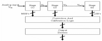
Figure 1 shows the block diagram of the Pipelined ADC system [1], which may be described as a number of cascaded stages each produces a low number of bits and then produce a residue signal to be processed by the following stage. Each digital output is then fed into the digital correction and calibration block to be synchronized and calibrated, then the output bits are fed into the output buffer.
Each stage (Figure 2) consists of a sample and hold, sub-ADC (Comparators), and MDAC.

Figure (1) Pipelined ADC

Figure (2) Pipelined Stage
2.2. 1.5 Bits/Stage stage Architecture
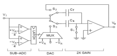
Figure 3 illustrates the switched capacitors circuit implementation of the 1.5 bits.
This architecture has been shown to be effective in achieving high throughout at low power [2].
The low number of bits per stage coupled with digital correction relaxes the constraint on comparator offset voltage and dc op-amp gain [3].

Figure( 3) 1.5 Bits/stage
The output voltage for each stage is specified according to the stage transfer function:

3. CIRCUITS NON-IDEALITIES
The target system is 10 bits pipelined ADC, with an ENOB of 9.5 Bits, without optimization we will consume a large area and power in our design but choosing optimum circuit spec¡¯s
In this section we are going to discuss for some circuits non-idealities in more details.
We have modeled the clock jitter effect in the sample and hold block, the comparators offset voltage, sampling capacitor thermal noise, capacitors mismatch, and for the OPAMP used in the MDAC we have modeled some of its non-idealities as finite dc gain, finite gain bandwidth product (GBW) and settling,
3.1 Sampling Uncertainty (Clock Jitter)
Clock jitter is the uncertainty in the value of the sampled signal due to uncertainty in the time of sampling, this effect can be modeled as an error voltage that depends on the slope of the signal and the jitter RMS [4] value (Gives a spec on the clock generation block).
Figure 4 [4] illustrate this model and figure 5 is the simulation results notice the vertical line which represents the sampling time value, we ¡¯ll choose the value of the jitter to be 15 psec (rms).

Figure (4) Clock Jitter Model
3.2 Comparators Offset
Applying the Random Sign Digit (RSD) technique has a very good impact on the offset voltage of the comparator. Theoretically for the 1.5 Bits/stage the digital correction block can tolerate an offset error till Vref / 4.
Figure 6 illustrates the model used for the comparator offset voltage as an offset to the comparison level.
Figure 7 is the simulation result which verifies our discussion as Vref = 0.8 V.
All stages may take the value of the offset voltage to be 50 mV to have a margin for the reference voltage variations and settling errors.

Figure (5) Clock Jitter Effect

Figure (6) Comparator Offset Model

Figure (7) Comparator Offset Effect
3.3 Sampling Capacitor Thermal Noise
The aim here is to find an optimum value for the capacitors for each stage.
For the sampling phase there is thermal noise due to the sampling capacitor, this value equals KT/Cs (Vrms2).
Figure 8 illustrates the way we are imbedding this source of noise to the signal [4].
Figure 9 is the simulation result from sweeping the value of the sampling capacitor and record the corresponding ENOB.
In fact the sampling capacitor value is limited to another property which is the capacitor mismatch (will be discussed later)
We may choose the value of the capacitor to be 0.8 pF

Figure (8) Sampling Capacitor Thermal Noise Model
3.4 Capacitors Mismatch
Capacitor mismatch impact may be represented in the transfer function by modifying the equation in [5] by setting A ![]() ¡Þ as:
¡Þ as:
![]()
Actually capacitor mismatch is inversely proportional to the capacitor¡¯s value.
Therefore the value of the capacitor should be the maximum value between the two values extracted from both thermal noise and capacitor mismatch.
Figure 10 is the simulation results for sweeping the value of the mismatch to record its impact on the ENOB.

Figure (9) Sampling Capacitor Thermal Noise
We¡¯ll choose the value of the mismatch to be 0.1 %.
This implies about 1pF for the unit cap, and then we should choose the maximum value between the two values of the sampling capacitor which is 1pF.
Another important remark is that the effect of the sampling capacitor value according to both capacitor thermal noise and mismatch is not the same for all stages; hence a tapering factor [5] should be taken to resize the capacitors for the next stages.
3.5 Non-Ideal OPAMP
3.5.1 Finite DC Gain
The finite OPAMP dc gain impact may be represented in the transfer function as [5]:

Figure (10) Capacitor Mismatch Effect
Figure 11 shows the simulation results from sweeping the value of the DC Gain for the OPAMP and its impact to ENOB.
We will choose the value of the DC Gain to be 70 dB.


Figure (11) Finite DC Gain Effect
3.5.2 Finite Gain-Bandwidth Product (GBW) and Slew Rate (SR)
Finite GBW and SR were modeled in [4], and is illustrated in figure 12 as the slope of the signal is compared to the SR of the OPAMP and according to the result OPAMP will go in slewing and then in linear region, or it will go in the linear region directly, after the decision was taken the error voltage ¦Å was calculated.
Figure 13 shows the simulation results for the effect of the finite Gain-Bandwidth product, and figure 14 shows the simulation results for the effect of the finite slew rate.
Actually, finite GBW and SR is a direct spec on the current budget for the OPAMP. Their values should be optimally chosen as their impact on performance is critical and on the other hand their values directly related to the current of the gain stage (for GBW) and the output stage (for SR after knowing the load capacitor value).

Figure (12) Finite GBW and SR Model
4. NON-IDEAL SYSTEM
Our target in this paper was to find optimum spec¡¯s for the circuits for this design.
The ideal pipelined ADC system was modeled and then the non-idealities discussed were added to it.
Figure 15 shows the ideal system simulation results and the ENOB = 10.15 bits with an SNDR= 61 dB, After adding the non-ideal effects to the model and choosing the values (summarized in table 1) the non-ideal system simulation result is presented in figure 16 and the ENOB= 9.5 bits for SNDR= 59 dB, to have a margin of about 3 dB (0.5 ENOB) for the remaining non-idealities (Not modeled in this work).

Figure (13) Finite GBW Effect

Figure (14) Finite SR Effect

Figure (15) Ideal System

Figure (16) Non-Ideal System
Table 1 illustrate the extracted circuit spec¡¯s for the ADC
| Jitter (psec) (rms) | 15 |
| Comparator Offset (mV) | 50 |
| Sampling Capacitor (pF) | 1,0.5,0.25,0.13,0.13,0.13,0.13,0.13 |
| Finite DC Gain (dB) | 70,70,40,40,20,20,20,20 |
| Finite SR (V/µsec) | 80,80,60,60,50,50,50,50 |
| Finite GBW (MHz) | 80,80,60,60,50,50,50,50 |
5. CONCLUSION
A design automation methodology was presented to implement a 10 bits ADC with 9 ENOB, the most important circuit non-idealities were modeled and a suitable margin was left for other non-modeled ones.
Circuit level spec¡¯s were extracted from the system level and optimization was done to get more optimum values, tapering factor was taken into account to resize the stage in terms of power and area and according to the contribution of each stage to the performance.
6. ACKNOWLEDGMENT
This work was sponsored by Smart Wireless Systems (SWS).
I would like to thank Prof.Dr. Hisham Hadara for his support, continuous guidance, and encouragement.
Also I would like to thank Dr. Ayman M. El-Sayed for his help, encouragement, and patience.
7. REFERENCES
[1] L. Sumanen, ¡°Pipelined Analog-to-Digital Converters for Wide-Band Wirekess Communications,¡± PHD Thesis, Nov.2002.
[2] Abo Thesis ¡°Design for reliability of low voltage, switched capacitor circuits, ¡° UC-Berkeley.
[3] H. Yu, X. Gong, J. Hung, ¡°A low power 10 bits 80 MS/s pipelined ADC.
[4] P. Malcovati, S. Brigati, F. Francesconi, F. Maloberti, P. Cusinato, A. Baschirotto, ¡°Behavioral Modeling of Switched-capacitor sigma-delta modulators,¡± IEEE Trans. Circuits Syst. I, vol.50, pp. 352¨C364, Mar. 2003
[5] P. Malcovati, S. Brigati, F. Francesconi, F. Maloberti, P. Cusinato, A. Baschirotto, ¡°A cost-efficient high-speed 12-bit pipelined ADC in 0.18-µm digital CMOS,¡± IEEE J. Solid-State Circuits, vol.40, pp. 1506¨C1513, July. 2005
