By Adelmario Douglas, Renata Bezerra, Diogo Maciel, Antonyus Pyetro, Edna Barros
Federal University of Pernambuco
Recife, Brazil
Abstract :
This paper presents a based on behavioral synthesis design flow that allows high-quality hardware and software design of IP-Cores. The main flow's advantage is that it allows hardware and software to be developed concurrently, reducing design time. This approach has been applied on the design of an USB[4] Host IP-core and its device driver. As a result, the IP-Core has been prototyped in an Altera® platform with the driver running on a NiosII processor.
1. Introduction
Due to the market’s pressures, the industry has increased the use of IP-Cores in digital systems design. On the other hand, the complexity of the IP-cores has also increased significantly, because, they often are needed to implement more functionalities, new protocols and different operation modes [8]. Moreover, in many cases, the IP core design includes some software development.
Due to this complexity, starting and IP-core design from an RTL specification increases the codification and verification time and, consequently, increasing the time to market. In particular, a critical point is the delay in software development. Thus, the increase of the development’s total time (hardware + software) is presented as a great challenge in the design of IP-cores.
A solution to reduce the IP-core development time is to describe it in a higher abstraction level, for faster IP modeling and earlier software development, and to use high level synthesis techniques to speed the FPGA or ASIC prototyping. Thus, this work proposes a design flow based on behavioral synthesis, which allows hardware and software concurrent development.
This project flow has been applied to the design of an USB host controller, and the development of its respective device driver. USB systems have become popular due to their flexibility and connection facilities, and they are present in the great majority of embedded systems.
This article is organized as follows: the section two shows the proposed design flow for IP-cores development. Section 3 explains the USB Host IP-Core structure used as case study. Section 4 explains the USB Host IP-core architecture developed in this work. Section 5 shows how the IP-core has been developed, and the section 6 shows how the prototyping has been obtained. Finally, section 7 presents some results, conclusions and future works.
2. The Proposed Design Flow
The USB Host Ip-core design has been done according to the ipPROCESS methodology [1][7], which has been already used in other IP-cores development [2].
In short, the ipPROCESS methodology (or IPP methodology) is a rigorous and thorough engineering process that guides designers through the design process, so that they can acquire a clear and unique understanding of the IP-core functionality and behavior. It has been inspired on the combination of well-known software engineering methodologies, like RUP [10] and XP [12], with IC design standards like VSIA [11] and RMM [13].
IPP defines the IP-core design task as a set of activities, where each activity determines “what should be done, when and by whomâ€, i.e., the process assigns activities and responsibilities to the right person at a right moment of the design life cycle. In IPP, the life cycle design of an IP-core starts in the Conception phase by eliciting requirements and constraints. After that the IP-core structure, functionalities and behavior should be defined during the Architecture phase. In this phase, the structure, functionalities and behavior are modeled using UML and Real Time UML [14]. Only after that, HDL design takes place. Due to the increasing IP-core complexity it is very important that the design team acquires a clear and unique understanding of the IP-core functionality and behavior, before any design refinement start.
The following phase is the RTL Design. It aims at producing an RTL specification of the IP in some hardware description language. This phase starts with a behavioral SystemC/C++ description, which is refined down to structural SystemC RTL and synthesized. Refinement can be done manually or automatically, by using some synthesis tool.
Concurrently with the RTL implementation, functional verification must take place in order to assure that the SystemC RTL description has the same behavior as the original (behavioral SystemC/C++) Reference Model (RM). The last phase is the Physical Prototyping phase, which aims at producing a running FPGA prototype.
By defining all these phases as a set of well defined activities, with actors and roles, we improve the design productivity, due to: (a) the increase in the probability of earlier error detection since the design starts at a higher level of abstraction; and (b) the continuous co-verification checks enabled by the adoption of a refinement strategy based on a single design language (SystemC).
Moreover, the designer knowledge of the design improves, since IPP makes the design activities more predictable, clarifying the abilities required to execute each one of the phases. The design time is recorded at each phase, so the process can be refined and calibrated for future designs.
As said before, IPP has been defined based on two software processes: RUP and XP. The main idea is to re-use and adapt the expertise in designing large software systems, accumulated over the years in the Software Engineering area, to a hardware workflow.
From these methodologies Rules and Practices that enforce quality have been adopted, which supports to start the design at a very high abstraction level. This is particularly useful to an ESL-based methodology, given that it allows the detection of errors at earlier design phases, while assures the quality of the final implementation.
Figure 1 shows an overview of the application of IPP. It has two dimensions: the horizontal axis represents time and shows the lifecycle aspects of the process, and the vertical axis represents disciplines, which group activities logically according to their nature.
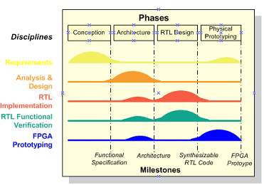
Figure 1: IPP Structure Overview
The first dimension represents the dynamic aspect of the process, i.e. how activities are distributed over the time. It is expressed in terms of Phases and Milestones. The second dimension represents the structural aspects of the process: how it is described in terms of disciplines, workflows, activities, artifacts and roles. The figure shows how the emphasis on one activity can vary over time.
By taking the ipPROCESS as reference, the proposed methodology starts from a behavioral description instead of a RTL specification. Another feature is the development of the device driver. Figure 2 shows the considered development flow for IP-cores design.
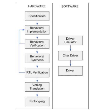
Figure 2– Development flow
The flow starts with the requisites elicitation and architecture definition during specification phase. Based on the architecture, the hardware and a module, which simulates the system software, are implemented, both at behavioral level.
The behavioral model is verified and, if no errors are found, the behavioral synthesis is performed. It transforms the behavioral specification into a RTL description. If any error is found, it must be fixed and the RTL description verified again. The way as the model is verified will be explained later.
In the RTL specification the same stimuli vectors are applied as in the behavioral level, if any error is found, corrections must be done in the behavioral and RTL specification. After correcting the errors, the complete set of stimuli vectors must be applied again.
Once the RTL code is verified, it is translated to Verilog language. This Verilog code is tested in the same way as described for the other levels, and the errors found and fixed in all descriptions starting from at behavioral level. After the code fixing, the logical synthesis and the prototyping are performed.
In this phase of the design, the found errors are, in the most cases, related to the directives used by the RTL synthesis tool, and not to the model logic. These directives are used to inform to the tool how to handle with ports delay or how to do the modules scheduling, for example.
In parallel to the hardware development, the related software is developed. It is usually a device driver that controls the device. The software’s first version is the Driver Emulator, a model described in some HDL, which simulates the system software behavior and is used to verify the hardware. The Char Driver is a driver code that tests only the interface, it is built based on the Driver Emulator. It is generally a code written in C/C++ that runs on a processor without an operating system. After the Char Driver validation, which has been done together with the controller, the operating system support can be added to the system. With this, the system’s software is ready, together with the hardware.
3. The Design of an USB Host Controller IP-core
The USB Host is formed by software and hardware. The software that controls the hardware and provide information to the OS, in this project, is called HCD (Host Controller Driver) and the hardware is called HC (Host Controller).
The HCD provides, to the system higher level, an interface to access the hardware functionalities. The access to HCD resources is usually made trough another driver, which is operating system dependent, called USBD. The HCD behavior is described in the USB specifications and follows the USB 2.0 standard. The hardware module HC is responsible for implementing the USB 2.0 protocol, communicating with the electrical interface and checking the data correctness. The HC is also based on the USB 2.0 standard. The complete USB System is composed by layers, from the operating system until the device, as shown in Figure 3.
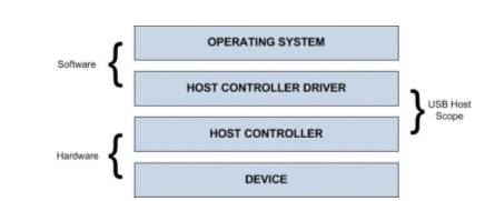
Figure 3– USB System layers
The communication between HCD and HC is made following a standard interfacing such as OHCI, EHCI or UHCI. In this design, the OHCI standard has been used. And the communication between HC and the device is made through the USB3300 electric interface [3], according to the OLPI’s communication protocol [5].
4. Host Controller Development
In the USB Host development, the HC has been divided in smaller modules, due to its complexity. Each one has been described in SystemC at behavioral level, and verified separately before being integrated to the HC. Most of the communication among the modules has been done at pin-accurate level, using FIFOs for the data channel implementation. Figure 4 shows in a very simplified way, the main sub-modules composing the HC module and its data channel.
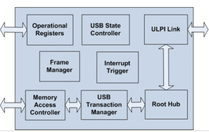
Figure 4 - HC Architecture
The connections between the modules are not showed in the figure. The HCD (a software module) exchanges information with the HC (a hardware module) through two interfaces: the Operational Registers and the Memory Access Controller slave and master respectively. Additionally, the HC communicates with the electrical interface through the ULPI Link.
The Operational Registers is a register bank that receives commands from the HCD and informs the HC status including information about interruptions, transmissions and devices. The Memory Access Controller is the module that does the read requests to the memory, came from the HC sub-modules.
The Frame Management is the sub-module, which handles the frame timing. As the transmissions must occur into time frames, the Frame Management notices the internal sub-modules when the frame starts or ends. The time of a frame is 1ms according to the USB specification. The USB State Controller takes care of the USB states, which can be: USBSuspend, USBResume, USBOperational and USBReset. These states were defined, mainly, to save power on HC (suspend state) and to synchronize the modules after reset (reset state). The Interrupt Trigger sub-module is in charge of informing to the HCD that a transaction has been accomplished. The information about the transactions stays in a memory area shared by HC and HCD. The sub-modules USB Transaction, Root Hub and ULPI Link are the modules that deal with the data transmission, in accordance with the USB protocol. Moreover, these are the sub-modules, which verify the transmitted data correctness and manage the USB protocol.
The HC design included four phases, as mentioned previously, before the prototyping. Just to remember, these phases were: specification, behavioral synthesis, verilog translation and logical synthesis. The verification performed after each of these phases has covered the correctness of a data transmission through the HC data channel, as well as the correctness of the USB protocol. To accomplish this verification, more two HDL modules have been included in our testbench: the HCD emulator (Driver Emulator) and the USB3300emulator (simulates the electrical interface).
Figure 5 shows the test-bench structure for the HC verification, and how the HCD and USB3300 emulators are connected to the HC.
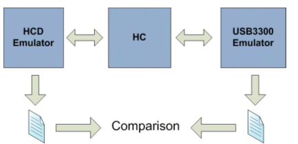
Figure 5 - Structure of Verification
The verification has been done analyzing the files transmitted trough the HC. Such files may come from HCD emulator or USB3300 emulator. The transmitted data values, as well as the order and the type of tokens that must be sent by the protocol, are stored in files that, at the end of the simulation, are compared with already known values (golden files). If the data values are different, an error is found.
The main aim of the tests is to validate the data channel, previously shown in Figure 4, and the USB protocol. A total of 61 channel tests combined with 24 protocol tests have been performed, totalizing 1464 test vectors. The same test structure has been used to the HC verification in all abstraction levels: behavioral, RTL and Verilog.
The behavioral synthesis and the tests simulation have been done through the use of Forte® Cynthesizer tool. The verilog translation has been also done using the Cynthesizer tool and the simulation using the VCS verification library. The logical synthesis has been done using the Cynthesizer tool and the Quartus tool, from Altera®, has been used for FPGA prototyping.
5 The Host Controller Driver Development
For the Host Controller Driver development an incremental process has been adopted. Such strategy was interesting because it has allowed handling the HCD complexity in a gradual way, as well as it has allowed developing software development while the controller was not finished.
The HCD implementation included four phases: creating an application, the development of the OHCI-driver in C for validating the OHCI interface; and the development of the HCD driver in C to emulate the HCD without OS; and finally, the port adaptation for the uClinux HCD. After that, the assembly of an USB device hardwired to the Host has been done through the Nios II Shell interface.
In the first phase, a simple application written in C language for the Nios II processor has been developed. This application had the objective of validating the reading and the writing of OHCI registers, testing the writing restrictions of some register’s bits, as the Interrupt Enable register, for example, where writing 1 has the effect of clearing that bit and writing 0 has no effect. In the second phase, a more complete application for HCD behavior emulation has been developed to validate the HC behavior. The HCD emulator is translated to a C code that validates the hardware interface. In the third phase, the HCD emulator has been replaced by uClinux [9] kernel, and some modifications must be done in the uClinux driver to better satisfy the OHCI specification. One of them had the objective to manage the Root Hub interruptions, that inform about the modifications occurred on the Root Hub ports and on the device.
6 Integration and Prototyping
For the HCD and HC integration, a platform including a memory, a Nios II processor and an Avalon bus, has been developed. This platform has been prototyped in a Stratix II EP2S60F672 FPGA [6] prototyping board and occupies 54% of the total area, with the HC occupying about 48%. The FPGA based platform including the USB Host is shown in Figure 6.
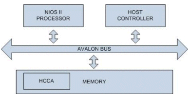
Figure 6 - USB System Architecture
The HCCA is a shared memory used to exchange information between HC (hardware) and the HCD.(software) modules. The HCD is running in the NIOS processor. The memory area is allocated by the HCD at the initialization and its address is stored in one of the HC registers, usually the HCCA stores information about the transmissions status.
7 Results and Conclusions
Besides the methodology for developing an IP-core and its driver concurrently, the main result of this work is an USB Host functional model prototyped in FPGA, which is able to operates in two distinct transmission types: control and bulk. Table 1 shows results related to the implementation.
Table 1 - USB Design results
Test vectors covering the two implemented transmission types have been executed in HC. Table 2 shows the simulation time spent to accomplish the test vectors at different abstraction levels.
Table 2 - Simulation Time
The table shows the simulation time for two protocol tests, each one executing all the channel tests in different abstraction levels : Behavioral and Verilog. Ack is the ideal flow protocol test, where the HC receives only ACK tokens. Timeout 3 is the test where the Timeout token is issued three times in the same transmission. The tests have been performed in a machine with the following configuration: AMD Sempron(tm) Processor +2800, 1GByte with CentOS Operating System.
As conclusion we can mention that the proposed methodology has been successfully used for the design of a complex IP-core including hardware and software design. The methodology is being integrated into the ipPROCESS.
References
[1] ipPROCESS, development process for Soft-IP, http://www.lincs.org.br/ipprocess (accessed September 25, 2007).
[2] A. K. Rocha, P. Lira, Y. Y. Ju, E. Barros, E. Melcher and G. Araujo, Silicon Validated Ip Cores Designed by the Brazil-IP Network, IP/Soc 2006.
[3] USB3300, electrical interface information, http://www.smsc.com/main/catalog/usb3300.html (last accessed in September 28, 2007).
[4] COMPAQ; HEWLETT-PACKARD; INTEL; LUCENT; MICROSOFT; NECK; PHILIPS. Universal Serial Bus Specification. Revision 2.0. April, 2000.
[5] PHILIPS; SMSC; TRANSDIMENSION, INC; MENTOR GRAPHICS CORPORATION; CONEXANT SYSTEMS,INC; ARC INTERNATIONAL INC. UTMI+ Low Pin Interface Specification. October, 2004.
[6] ALTERA. Stratix II Handbook, Volume 1 and 2. May, 2007.
[7] Lima, Marília. “ipProcess : Um Processo de Desenvolvimento de Módulos de Propriedade Intelectual com Implementação em FPGA´sâ€. MSc Dissertation in Computer Science, Informatics Centre, UFPE. 2005.
[8] Nacul A., Lajolo M., Givargis T.: Interface-Centric Abstraction level for Rapid Hardware/Software Integration, Book Chapter in Application of Specification and Design Languages for SOCs. Springer, (2006)
[9] Microtronix WebSite, http://www.microtronix.com (last accessed in October 28, 2007)
[10] P. Krutchen, The Rational Unified Process, Addison-Wesley, 1998.
[11] VSIA: Virtual Socket Interface Alliance, Available at: http://www.vsia.org.
[12] eXtreme Programming, Available at: http://www.extremeprogramming.org, 2006.
[13] M. Keating, P. Bricaud, Reuse Methodology Manual for System-on-chip Design, Kluwer Academic Publishers, 2002.
[14] U2 Partners, OMG RFPs ad/00-90-01 and ad/00-09-02, Unified Modeling Language 2.0, Version 0.671.
Federal University of Pernambuco
Recife, Brazil
Abstract :
This paper presents a based on behavioral synthesis design flow that allows high-quality hardware and software design of IP-Cores. The main flow's advantage is that it allows hardware and software to be developed concurrently, reducing design time. This approach has been applied on the design of an USB[4] Host IP-core and its device driver. As a result, the IP-Core has been prototyped in an Altera® platform with the driver running on a NiosII processor.
1. Introduction
Due to the market’s pressures, the industry has increased the use of IP-Cores in digital systems design. On the other hand, the complexity of the IP-cores has also increased significantly, because, they often are needed to implement more functionalities, new protocols and different operation modes [8]. Moreover, in many cases, the IP core design includes some software development.
Due to this complexity, starting and IP-core design from an RTL specification increases the codification and verification time and, consequently, increasing the time to market. In particular, a critical point is the delay in software development. Thus, the increase of the development’s total time (hardware + software) is presented as a great challenge in the design of IP-cores.
A solution to reduce the IP-core development time is to describe it in a higher abstraction level, for faster IP modeling and earlier software development, and to use high level synthesis techniques to speed the FPGA or ASIC prototyping. Thus, this work proposes a design flow based on behavioral synthesis, which allows hardware and software concurrent development.
This project flow has been applied to the design of an USB host controller, and the development of its respective device driver. USB systems have become popular due to their flexibility and connection facilities, and they are present in the great majority of embedded systems.
This article is organized as follows: the section two shows the proposed design flow for IP-cores development. Section 3 explains the USB Host IP-Core structure used as case study. Section 4 explains the USB Host IP-core architecture developed in this work. Section 5 shows how the IP-core has been developed, and the section 6 shows how the prototyping has been obtained. Finally, section 7 presents some results, conclusions and future works.
2. The Proposed Design Flow
The USB Host Ip-core design has been done according to the ipPROCESS methodology [1][7], which has been already used in other IP-cores development [2].
In short, the ipPROCESS methodology (or IPP methodology) is a rigorous and thorough engineering process that guides designers through the design process, so that they can acquire a clear and unique understanding of the IP-core functionality and behavior. It has been inspired on the combination of well-known software engineering methodologies, like RUP [10] and XP [12], with IC design standards like VSIA [11] and RMM [13].
IPP defines the IP-core design task as a set of activities, where each activity determines “what should be done, when and by whomâ€, i.e., the process assigns activities and responsibilities to the right person at a right moment of the design life cycle. In IPP, the life cycle design of an IP-core starts in the Conception phase by eliciting requirements and constraints. After that the IP-core structure, functionalities and behavior should be defined during the Architecture phase. In this phase, the structure, functionalities and behavior are modeled using UML and Real Time UML [14]. Only after that, HDL design takes place. Due to the increasing IP-core complexity it is very important that the design team acquires a clear and unique understanding of the IP-core functionality and behavior, before any design refinement start.
The following phase is the RTL Design. It aims at producing an RTL specification of the IP in some hardware description language. This phase starts with a behavioral SystemC/C++ description, which is refined down to structural SystemC RTL and synthesized. Refinement can be done manually or automatically, by using some synthesis tool.
Concurrently with the RTL implementation, functional verification must take place in order to assure that the SystemC RTL description has the same behavior as the original (behavioral SystemC/C++) Reference Model (RM). The last phase is the Physical Prototyping phase, which aims at producing a running FPGA prototype.
By defining all these phases as a set of well defined activities, with actors and roles, we improve the design productivity, due to: (a) the increase in the probability of earlier error detection since the design starts at a higher level of abstraction; and (b) the continuous co-verification checks enabled by the adoption of a refinement strategy based on a single design language (SystemC).
Moreover, the designer knowledge of the design improves, since IPP makes the design activities more predictable, clarifying the abilities required to execute each one of the phases. The design time is recorded at each phase, so the process can be refined and calibrated for future designs.
As said before, IPP has been defined based on two software processes: RUP and XP. The main idea is to re-use and adapt the expertise in designing large software systems, accumulated over the years in the Software Engineering area, to a hardware workflow.
From these methodologies Rules and Practices that enforce quality have been adopted, which supports to start the design at a very high abstraction level. This is particularly useful to an ESL-based methodology, given that it allows the detection of errors at earlier design phases, while assures the quality of the final implementation.
Figure 1 shows an overview of the application of IPP. It has two dimensions: the horizontal axis represents time and shows the lifecycle aspects of the process, and the vertical axis represents disciplines, which group activities logically according to their nature.

Figure 1: IPP Structure Overview
The first dimension represents the dynamic aspect of the process, i.e. how activities are distributed over the time. It is expressed in terms of Phases and Milestones. The second dimension represents the structural aspects of the process: how it is described in terms of disciplines, workflows, activities, artifacts and roles. The figure shows how the emphasis on one activity can vary over time.
By taking the ipPROCESS as reference, the proposed methodology starts from a behavioral description instead of a RTL specification. Another feature is the development of the device driver. Figure 2 shows the considered development flow for IP-cores design.

Figure 2– Development flow
The flow starts with the requisites elicitation and architecture definition during specification phase. Based on the architecture, the hardware and a module, which simulates the system software, are implemented, both at behavioral level.
The behavioral model is verified and, if no errors are found, the behavioral synthesis is performed. It transforms the behavioral specification into a RTL description. If any error is found, it must be fixed and the RTL description verified again. The way as the model is verified will be explained later.
In the RTL specification the same stimuli vectors are applied as in the behavioral level, if any error is found, corrections must be done in the behavioral and RTL specification. After correcting the errors, the complete set of stimuli vectors must be applied again.
Once the RTL code is verified, it is translated to Verilog language. This Verilog code is tested in the same way as described for the other levels, and the errors found and fixed in all descriptions starting from at behavioral level. After the code fixing, the logical synthesis and the prototyping are performed.
In this phase of the design, the found errors are, in the most cases, related to the directives used by the RTL synthesis tool, and not to the model logic. These directives are used to inform to the tool how to handle with ports delay or how to do the modules scheduling, for example.
In parallel to the hardware development, the related software is developed. It is usually a device driver that controls the device. The software’s first version is the Driver Emulator, a model described in some HDL, which simulates the system software behavior and is used to verify the hardware. The Char Driver is a driver code that tests only the interface, it is built based on the Driver Emulator. It is generally a code written in C/C++ that runs on a processor without an operating system. After the Char Driver validation, which has been done together with the controller, the operating system support can be added to the system. With this, the system’s software is ready, together with the hardware.
3. The Design of an USB Host Controller IP-core
The USB Host is formed by software and hardware. The software that controls the hardware and provide information to the OS, in this project, is called HCD (Host Controller Driver) and the hardware is called HC (Host Controller).
The HCD provides, to the system higher level, an interface to access the hardware functionalities. The access to HCD resources is usually made trough another driver, which is operating system dependent, called USBD. The HCD behavior is described in the USB specifications and follows the USB 2.0 standard. The hardware module HC is responsible for implementing the USB 2.0 protocol, communicating with the electrical interface and checking the data correctness. The HC is also based on the USB 2.0 standard. The complete USB System is composed by layers, from the operating system until the device, as shown in Figure 3.

Figure 3– USB System layers
The communication between HCD and HC is made following a standard interfacing such as OHCI, EHCI or UHCI. In this design, the OHCI standard has been used. And the communication between HC and the device is made through the USB3300 electric interface [3], according to the OLPI’s communication protocol [5].
4. Host Controller Development
In the USB Host development, the HC has been divided in smaller modules, due to its complexity. Each one has been described in SystemC at behavioral level, and verified separately before being integrated to the HC. Most of the communication among the modules has been done at pin-accurate level, using FIFOs for the data channel implementation. Figure 4 shows in a very simplified way, the main sub-modules composing the HC module and its data channel.

Figure 4 - HC Architecture
The connections between the modules are not showed in the figure. The HCD (a software module) exchanges information with the HC (a hardware module) through two interfaces: the Operational Registers and the Memory Access Controller slave and master respectively. Additionally, the HC communicates with the electrical interface through the ULPI Link.
The Operational Registers is a register bank that receives commands from the HCD and informs the HC status including information about interruptions, transmissions and devices. The Memory Access Controller is the module that does the read requests to the memory, came from the HC sub-modules.
The Frame Management is the sub-module, which handles the frame timing. As the transmissions must occur into time frames, the Frame Management notices the internal sub-modules when the frame starts or ends. The time of a frame is 1ms according to the USB specification. The USB State Controller takes care of the USB states, which can be: USBSuspend, USBResume, USBOperational and USBReset. These states were defined, mainly, to save power on HC (suspend state) and to synchronize the modules after reset (reset state). The Interrupt Trigger sub-module is in charge of informing to the HCD that a transaction has been accomplished. The information about the transactions stays in a memory area shared by HC and HCD. The sub-modules USB Transaction, Root Hub and ULPI Link are the modules that deal with the data transmission, in accordance with the USB protocol. Moreover, these are the sub-modules, which verify the transmitted data correctness and manage the USB protocol.
The HC design included four phases, as mentioned previously, before the prototyping. Just to remember, these phases were: specification, behavioral synthesis, verilog translation and logical synthesis. The verification performed after each of these phases has covered the correctness of a data transmission through the HC data channel, as well as the correctness of the USB protocol. To accomplish this verification, more two HDL modules have been included in our testbench: the HCD emulator (Driver Emulator) and the USB3300emulator (simulates the electrical interface).
Figure 5 shows the test-bench structure for the HC verification, and how the HCD and USB3300 emulators are connected to the HC.

Figure 5 - Structure of Verification
The verification has been done analyzing the files transmitted trough the HC. Such files may come from HCD emulator or USB3300 emulator. The transmitted data values, as well as the order and the type of tokens that must be sent by the protocol, are stored in files that, at the end of the simulation, are compared with already known values (golden files). If the data values are different, an error is found.
The main aim of the tests is to validate the data channel, previously shown in Figure 4, and the USB protocol. A total of 61 channel tests combined with 24 protocol tests have been performed, totalizing 1464 test vectors. The same test structure has been used to the HC verification in all abstraction levels: behavioral, RTL and Verilog.
The behavioral synthesis and the tests simulation have been done through the use of Forte® Cynthesizer tool. The verilog translation has been also done using the Cynthesizer tool and the simulation using the VCS verification library. The logical synthesis has been done using the Cynthesizer tool and the Quartus tool, from Altera®, has been used for FPGA prototyping.
5 The Host Controller Driver Development
For the Host Controller Driver development an incremental process has been adopted. Such strategy was interesting because it has allowed handling the HCD complexity in a gradual way, as well as it has allowed developing software development while the controller was not finished.
The HCD implementation included four phases: creating an application, the development of the OHCI-driver in C for validating the OHCI interface; and the development of the HCD driver in C to emulate the HCD without OS; and finally, the port adaptation for the uClinux HCD. After that, the assembly of an USB device hardwired to the Host has been done through the Nios II Shell interface.
In the first phase, a simple application written in C language for the Nios II processor has been developed. This application had the objective of validating the reading and the writing of OHCI registers, testing the writing restrictions of some register’s bits, as the Interrupt Enable register, for example, where writing 1 has the effect of clearing that bit and writing 0 has no effect. In the second phase, a more complete application for HCD behavior emulation has been developed to validate the HC behavior. The HCD emulator is translated to a C code that validates the hardware interface. In the third phase, the HCD emulator has been replaced by uClinux [9] kernel, and some modifications must be done in the uClinux driver to better satisfy the OHCI specification. One of them had the objective to manage the Root Hub interruptions, that inform about the modifications occurred on the Root Hub ports and on the device.
6 Integration and Prototyping
For the HCD and HC integration, a platform including a memory, a Nios II processor and an Avalon bus, has been developed. This platform has been prototyped in a Stratix II EP2S60F672 FPGA [6] prototyping board and occupies 54% of the total area, with the HC occupying about 48%. The FPGA based platform including the USB Host is shown in Figure 6.

Figure 6 - USB System Architecture
The HCCA is a shared memory used to exchange information between HC (hardware) and the HCD.(software) modules. The HCD is running in the NIOS processor. The memory area is allocated by the HCD at the initialization and its address is stored in one of the HC registers, usually the HCCA stores information about the transmissions status.
7 Results and Conclusions
Besides the methodology for developing an IP-core and its driver concurrently, the main result of this work is an USB Host functional model prototyped in FPGA, which is able to operates in two distinct transmission types: control and bulk. Table 1 shows results related to the implementation.
Table 1 - USB Design results
| Results | |
| Requirements | 147 |
| Architecture | 12 modules |
| Source Code | 9158 code lines |
| Testbench | 16400 code lines |
| Prototyping | 20599 ALUS |
Test vectors covering the two implemented transmission types have been executed in HC. Table 2 shows the simulation time spent to accomplish the test vectors at different abstraction levels.
Table 2 - Simulation Time
| Protocol Test | Behavioral | Verilog |
| ACK | 53m54s | 110m26s |
| TIMEOUT 3 | 69m23s | 143m0s |
The table shows the simulation time for two protocol tests, each one executing all the channel tests in different abstraction levels : Behavioral and Verilog. Ack is the ideal flow protocol test, where the HC receives only ACK tokens. Timeout 3 is the test where the Timeout token is issued three times in the same transmission. The tests have been performed in a machine with the following configuration: AMD Sempron(tm) Processor +2800, 1GByte with CentOS Operating System.
As conclusion we can mention that the proposed methodology has been successfully used for the design of a complex IP-core including hardware and software design. The methodology is being integrated into the ipPROCESS.
References
[1] ipPROCESS, development process for Soft-IP, http://www.lincs.org.br/ipprocess (accessed September 25, 2007).
[2] A. K. Rocha, P. Lira, Y. Y. Ju, E. Barros, E. Melcher and G. Araujo, Silicon Validated Ip Cores Designed by the Brazil-IP Network, IP/Soc 2006.
[3] USB3300, electrical interface information, http://www.smsc.com/main/catalog/usb3300.html (last accessed in September 28, 2007).
[4] COMPAQ; HEWLETT-PACKARD; INTEL; LUCENT; MICROSOFT; NECK; PHILIPS. Universal Serial Bus Specification. Revision 2.0. April, 2000.
[5] PHILIPS; SMSC; TRANSDIMENSION, INC; MENTOR GRAPHICS CORPORATION; CONEXANT SYSTEMS,INC; ARC INTERNATIONAL INC. UTMI+ Low Pin Interface Specification. October, 2004.
[6] ALTERA. Stratix II Handbook, Volume 1 and 2. May, 2007.
[7] Lima, Marília. “ipProcess : Um Processo de Desenvolvimento de Módulos de Propriedade Intelectual com Implementação em FPGA´sâ€. MSc Dissertation in Computer Science, Informatics Centre, UFPE. 2005.
[8] Nacul A., Lajolo M., Givargis T.: Interface-Centric Abstraction level for Rapid Hardware/Software Integration, Book Chapter in Application of Specification and Design Languages for SOCs. Springer, (2006)
[9] Microtronix WebSite, http://www.microtronix.com (last accessed in October 28, 2007)
[10] P. Krutchen, The Rational Unified Process, Addison-Wesley, 1998.
[11] VSIA: Virtual Socket Interface Alliance, Available at: http://www.vsia.org.
[12] eXtreme Programming, Available at: http://www.extremeprogramming.org, 2006.
[13] M. Keating, P. Bricaud, Reuse Methodology Manual for System-on-chip Design, Kluwer Academic Publishers, 2002.
[14] U2 Partners, OMG RFPs ad/00-90-01 and ad/00-09-02, Unified Modeling Language 2.0, Version 0.671.
