Silvia Dondi, Silis s.r.l.
Marco Bigi, Andrea Boni, Matteo Tonelli, Dipartimento di Ingegneria dell'Informazione - University of Parma
Abstract :
The current technology trend for Analog-to- Digital Converters (ADCs) is particularly keen on power reduction, together with high-speed performance. The goal of the paper is to demonstrate that both the features can be achieved by a time-interleaved ADC architecture exploiting Successive Approximation (SA) algorithm. A 6-bit time-interleaved SA-ADC for Ultra-Wide Band (UWB) applications is proposed. The converter, designed in 90nm General Purpose (GP) CMOS technology, exhibits a maximum sampling frequency of 1.2GHz at 1V supply with 500mV input range and 16mW of power consumption.
I . INTRODUCTION
ADCs have always played a key role in several application fields of the communications industry. In recent years, the importance of ADCs has been growing mainly due to the developments of the UWB system and Software Defined Radios (SDRs). Nevertheless, in the last 20 years the panorama has consistently changed. As a matter of fact, the requirements for resolution improvements has slowed down, while the demand for higher sampling speeds keeps increasing. Finally, power reduction has become the major challenge in ADCs design [1].
The purpose of this work is presenting a novel ADC architecture for high-speed, low-to-moderate resolution and very-low power applications. Flash ADCs used to be the traditional architecture matching the requests above [2]. However, portable devices call for power-saving solutions that, together with a sampling frequency in the GHz range raises tremendous design issues. A feasible compromise is represented by Successive Approximation (SA) conversion, since it uses only one latch-comparator as analog part along with simple digital logics and a switching network to implement a binary search algorithm [3].
The present project aimed at achieving a verylow power consumption at a sampling rate compatible with UWB receivers and incoming DVD player (1.2GS/s), still maintaining an effective resolution higher than 5-b under Nyquist conditions. So far there have not been reports in literature on ADCs showing contemporaneously such ambitious performance in speed and consumption for 90nm CMOS. As a matter of fact, the time-interleaved SA-ADC reported in [4] features a sampling speed lower than 1GS/s, while in [5] an ultra-low power consumption is obtained at the cost of a very a low (less than 4-b) effective resolution under full-Nyquist conditions. The ADC based on a subranging/parallel architecture presented in [6] can be considered as the state-of-the-art for such resolution and frequency.
The novel time-interleaved SA-ADC in 90nm technology proposed hereafter is proved to be more power-saving thanks to the predominant digital core over the analog circuits. In order to achieve highspeed, a strong effort in the customization of the digital part is absolutely unavoidable. In sect. II and III the basic architecture of a timeinterleaved SA-ADC is illustrated. In sect. IV the simulation results of the complete converter over the whole corner space are presented and discussed.
II. TIME-INTERLEAVED SA-ADC
The proposed time-interleaved SA-ADC architecture, shown in fig. 1, employes N+1 SAADC slices (N being the number of bit), while previous works required N+2 slices [4]. The absence of a front-end sample-and-hold section limits the power consumption and poses some constraints on the maximum clock skew among the interleaved slices (sect. IV). The selection of the ADC slice from which the digital output has to be provided is achieved through a mux driven by an encoder.
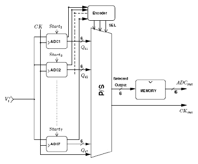
Fig. 1 Time-interleaved SA-ADC
III. SA-ADC SLICE
The classical SA-ADC is constituted by a Sample-and-Hold (S/H), a comparator (regenerative latch), a Digital-to-Analog Converter (DAC) and a Successive Approximation Register (SAR). In the current implementation, the S/H block is avoided since the sampling function is carried out within the DAC itself [3].
A. Switched-capacitor DAC with merging
The switched-capacitor DAC architecture in fig. 2 is fully differential and is based on the charge redistribution principle.
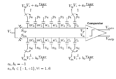
Fig. 2 Switched-capacitor DAC
Using a binary search algorithm that gradually halves the conversion range, the DAC output voltage successively approximates the differential input. The binary-search procedure lasts seven clock periods: the first one is required for sampling the input signal, while the others are actually the conversion steps. During the sampling phase, S1p and S1n are closed in order to allow Vp and Vn being connected to the common mode potential Vc. At the same time, the bottom plates of the capacitors are tied to the signal inputs Vip and Vin. Afterwards, S1p and S1n are opened, so the  MSB capacitors are connected to the positive reference:
 while the negative reference
 is fed to the remaining principle on both branches, the expressions for the potentials Vp and Vn, symmetrical around Vc, may be easily found.
The DAC linearity is severely affected by the common-mode switches, S1p and S1n, because of their on-resistance together with both charge sharing and charge injection effects. In the present design, a 6-b resolution at 1.2GS/s is achieved by resorting to gate voltage boosting which lowers the switch on-resistance while keeping a small transistor width.
In order to enhance DAC linearity, the mergedcapacitor technique [7] is exploited. The 64 capacitors of the 6-bit DAC are merged into 32 capacitors and contemporaneously the capacitive unit is doubled. As a consequence, power consumption and die area are not affected and a better matching is obtained. Since the capacitive unit is C0=50fF, the total DAC overall capacitance is 1.6pF.
B. Fully-synchronous SAR
This block implements the binary search algorithm and drives the DAC. The first solution investigated was inspired by Anderson [9] and is illustrated in fig. 3. It consists of N=6 JK-FFs used both as a shift-register and code-register, with K inputs fed by the comparator output.
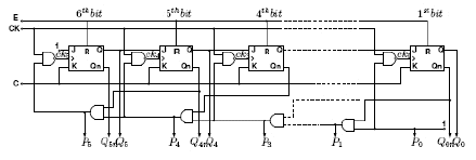
Fig. 3 Anderson's SAR
An internally generated signal resets all the JKFFs every seven clock periods. During the second clock period, the 6th JK-FF either toggles or is set, while the other JK-FFs are either in latch or in reset mode, so Q5=1 and Qi=0, i=0..4. On the third period, if K=1, meaning Vp>Vn, both 5th and 4th JKFFs toggle, so Q5=0 and Q4=1. On the other hand, if K=0, they are both in set state: Q5=1 and Q4=1. Signals Qi and Qin, with i=0..5 are then used to drive the DAC input. At each step from the 3rd to 7th two events occur: the current bit is set and the preceding bit is decided on the basis of the comparator output. The feedback signals Pi are high during the reset phase, then they gradually become low from the 6th to the 1st bit slice, as shown in fig. 4. When Pi goes low, the corresponding cki is forced in the high state and does not trigger anymore, causing the involved JK-FF to be disabled.
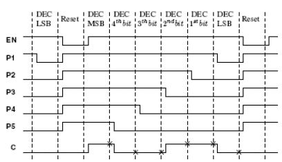
Fig. 4 SAR waveforms
In order to avoid the timing issues due to Anderson's asynchronous feedback, a novel fullysynchronous D-FFs SAR architecture was proposed in [8].
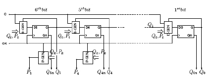
Fig. 5 Fully-synchronous SAR
The new solution, depicted in fig. 5, is based on a chain of D-FFs with synchronous feedback. All the D-FFs are designed as C2MOS master-slave logic without asynchronous reset and are triggered with the master clock in order to have the D-FFs sampling at the same time. The Di signals are generated by D-GEN block using some Qi and Pi signals (with i=0..5) as inputs. The delay between the master clock reference and the signals driving the DAC switches is minimized, allowing to achieve a clock frequency in the GHz range with a 90nm technology. Moreover, this provides benefits in terms of power consumption with respect to the JKFF SAR. Using an external data-register operating at the master clock frequency, the decision on the LSB is taken directly from the comparator output.
I V. SIMULATION RESULTS
In fig. 6-a the output spectrum of the timeinterleaved SA-ADC, designed in 90nm GP CMOS, is reported. The simulation refers to the worst-case corner of 1V supply, slow models and 85°C, assuming a 500mVpp input sine-wave at Nyquist condition (597MHz). The spectrum exhibits a SFDR higher then 45dB, a THD of -54.9dB and an overall SNDR compatible with more than 5.8 ENOB.
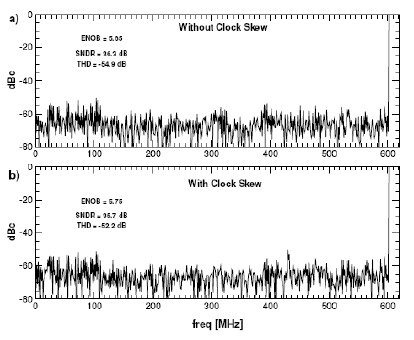
Fig. 6 Simulated spectrum of the ADC output
The effect of the timing skew occurring among the slice-array was also evaluated. As a matter of fact, timing skew is due to the routing of the clock lines, the threshold mismatch among the sampling switches and to the delay of the local clock buffers. From Monte-Carlo simulations and considering the chip floor-planning, the maximum skew is estimated within 3ps. Including such effect, the simulated ENOB is still higher than 5.7-b (fig. 6-b).
Furthermore, the mismatch occurring in the DAC capacitors due to random effects and layout parasitics was taken into account. Including a pessimistic mismatch of 1% in the capacitor array the converter exhibits a simulated effective resolution of 5.6-b at Nyquist. The layout of the chip, shown in fig. 7, presents a high degree of symmetry in order to minimize the timing skew and results in a very compact shape (1mm2 including the pads).The simulated performance of the interleaved ADC is summarized in tab. 1 and refers to the whole corner space. It is worth noticing that the power-saving feature is achieved mostly thanks to the proposed fully-synchronous SAR requiring only 1.3mA of current consumption. In addition, the proposed time-interleaved SA-ADC shows the lowest FOM (defined as ), evaluated at the maximum sampling speed under Nyquist condition. The experimental results are expected to be available soon since the chip is currently under packaging.
| Technology | 90nm GP CMOS |
| Supply Voltage | 1.2±0.2 V |
| Max Sampling Frequency | 1.2 GHz |
| Input Range (diff.) | 500 mV |
| ENOB (@ Nyquist) | 5.6-b |
| THD | -52 dB |
| DNL max | 0.2 LSB |
| FOM | 0.3 pJ/conv |
| Power Consumption (@ 1 V Supply) | 16 mW |
Tab. 1 Simulated performance of the proposed ADC
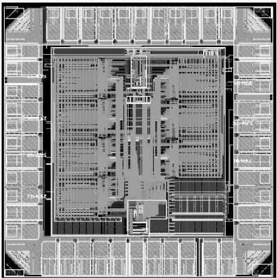
Fig. 7 Chip layout
V . CONCLUSION
The recent developments in modern communication industry is pushing the boundaries of ADCs. In this demanding scenary, an entirely custom 6-bit time-interleaved SA-ADC for ultrawide band applications, designed in 90nm GP CMOS, has been proposed. The novel solution, combining the benefits of time-interleaving and successive approximation structure, allows a significant power-saving basically achieved by the fully-synchronous SAR.
REFERENCES
[1] B. Le, T. W. Rondeau, J. H. Reed, C. W. Bostian, “Analog-to-Digital Convertersâ€, IEEE Signal Processing Magazine, Nov. 2004.
[2] C. Sandner et al. “A 6bit, 1.2 GSps Low-Power Flash-ADC in 0.13ìm Digital CMOSâ€, Proc. of IEEE ISSCC, 2004.
[3] J. Sauerbrey, D. Schmitt-Landsiedel, R. Thewes, “A 0.5-V 1-ì W Successive Approximation ADCâ€, IEEE JSSC, 38(7), July 2003.
[4] D. Draxelmayr, “A 6b 600MHz 10mW ADC Array in Digital 90nm CMOSâ€, Proc. of IEEE ISSCC, 2004.
[5] B.P. Ginsburg, A.P. Chandrakasan, “Dual Scalable 500MS/s, 5b Time-Interleaved SAR ADCs for UWB applicationsâ€, Proc. of IEEE CICC, 2005.
[6] P. Figureido et al., “A 90nm CMOS 1.2V 6b 1GS/s Two-Step Subranging ADCâ€, Proc. of IEEE ISSCC, 2006.
[7] Y.D. Jeon et al. “Acquisition-Time Minimization and Merged-Capacitor Switching Techniques for Sampling-Rate and Resolution Improvement of CMOS ADCsâ€, Proc. of IEEE ISCAS, May 2000.
[8] S. Dondi, D. Vecchi, A. Boni, M. Bigi, “A 6-bit, 1.2 GHz Interleaved SAR ADC in 90nm CMOSâ€, Proc. of IEEE Ph.D Research in Microelectronics and electronics, PRIME, 2006.
[9] T. O. Anderson, “Optimum Control Logic for Successive Approximation Analog-to-Digital Convertersâ€, JPL Technical Report, 32-1526, vol. XIII.
