Euhan Chong, Nelson Lam, Navraj Nandra, Zhinian Shu, Dino Toffolon
Synopsys
Abstract
This paper presents some key concepts necessary to design and build high-quality mixed-signal IP in 65‑nm or smaller geometries. The paper addresses design, layout, and verification techniques—with a focus on low-power design, reliability, and yield. Several design examples are presented, highlighting key techniques employed in the Synopsys® DesignWare® Mixed-Signal Intellectual Property (MSIP) portfolio.
I. Introduction
As processes continue to scale aggressively, deep sub-micron, mixed-signal design is becoming more challenging—especially when attempting to produce high-quality mixed-signal intellectual property (MSIP). Stress effects, increased leakage, smaller supply voltages, and reduced oxide thicknesses all make it extremely difficult to build low-power, long-lasting, and high-yielding mixed-signal IP. This paper discusses the three main factors often associated with MSIP: power, reliability, and yield, with a focus on design and verification flows to improve quality. Examples of MSIP includes the USB 2.0 PHY, ADC/DAC, PLL, SERDES (PCI Express®, SATA, XAUI), and DDR.
Section II of this paper presents an overview of some low-power design concepts and provides some examples of low-power circuits from the Synopsys DesignWare MSIP portfolio. This section describes some ultra-low-power techniques used in designs where very aggressive power reduction is necessary to enable integration into mobile applications.
Section III of the paper discusses some key stress effects found in deep sub-micron processes such as Hot Carrier Injection HCI, Negative Bias Temperature Instability (NBTI), and general gate oxide dielectric stress. This section presents design techniques that can be implemented in MSIP to help mitigate the impact on long-term analog circuit performance. This section includes an example of how to build high-voltage tolerant circuits using thinner oxide devices by employing clamping, cascoding, and regulation to reduce gate oxide stress. This section also presents a reliability flow that helps to better predict the MSIP’s long-term performance and reliability. This flow includes automated stress checks, and end-of-life and electro-migration (EM) simulations.
Finally, Section IV outlines some key techniques used to design MSIP with high manufacturability and production-level yield. This section discusses some key sources of mismtach that can ultimately impact yield. The concept of analog programmability is also introduced as a feature for optimizing yield in designs where process shifts require recentering of the design. This analog programmabilty is key to optimizing yield and reducing the need for costly respins.
II. Low-Power Design
Power—one of the most important factors in defining quality MSIP and lowering power consumption—must be considered early in the design phase. The following examples demonstrate several methods and architectures used in MSIP to minimize power—both in active and sleep/low-power modes.
The following is an example of a low-power, high-speed driver used in the Synopsys DesignWare USB 2.0 PHY. Power is kept very low with the use of a voltage-mode driver, shown in Fig.. 1. A voltage-mode driver draws 50% less current from the supply when compared to a conventional current-mode driver shown in Fig.. 2. In fact, for AC-coupled systems such as PCI Express®, SATA, and XAUI, a voltage-mode driver draws 25% of the supply current of a current-mode implementation. For example, a classical USB 2.0 driver requires nominal amplitude of 400 mV for high-speed data transmission into a 45-ohm load. The static power dissipation from the supply for a current-mode driver is:
 (1)
(1)
Whereas, the power dissipation from the supply for a voltage-mode driver is:
 (2)
(2)
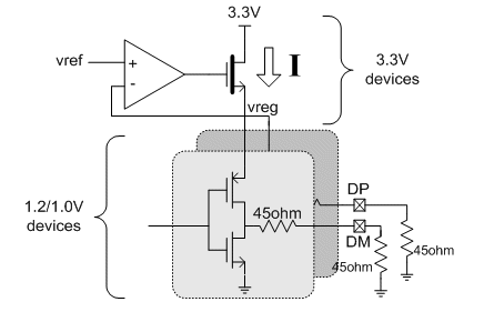
Fig. 1: Simplified Voltage Mode Driver Implemented in Synopsys DesignWare USB 2.0 PHY
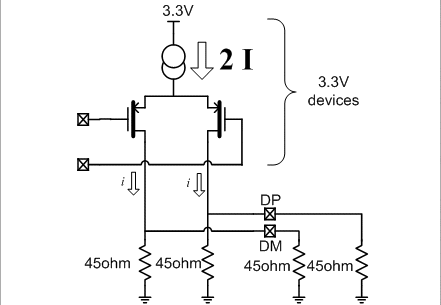
Fig. 2: Conventional USB 2.0 PHY Current-Mode Driver
Another power-reduction technique is shown in the DesignWare USB 2.0 PHY high-speed receive path (Fig. 3). Power is optimized by level shifting down into the low-voltage core device domain as early as possible in the signal path so that its device characteristics are leveraged as much as possible in order to reduce power. This strategy enables most high-frequency analog signal processing to be done in the low-voltage domain (for example, high-speed squelch detection and high speed receive function are implemented using low voltage core devices).
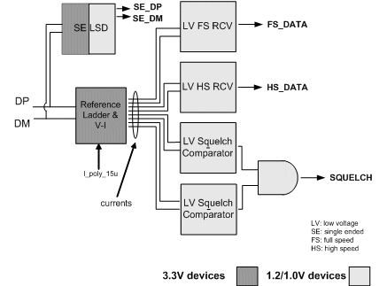
Fig. 3: Synopsys DesignWare USB 2.0 PHY Receiver Front End
Low-power design is also important in sleep modes (non-functional modes) especially for mobile devices. For example, in the USB protocol the PHY can be held in suspend mode for long periods of time. As a result the power dissipation in this mode can become a significant portion of the total and must be scaled aggressively.
Power gating in digital circuits is often used where more aggressive power reduction is necessary. Power gating helps reduce both channel and gate leakage by collapsing the supply and eliminating the leakage current path. This can be implemented on a sub-block level by implementing collapsible, thick-oxide regulators that can be disabled in low-power modes. These regulators are inherently used throughout MSIP design as shown in Fig 1. Digital supply leakage often dominates the power down current and so many SOC's collapse the digital (core) supply rail in these modes as well. Doing so can cause serious side-effects as analog level-shifters found in MSIP can often cause excessive current draw. Special care in the design of level shifters found in MSIP is necessary to avoid this. One example includes circuitry that detects when the digital power supply is collapsed; the circuitry then presets the analog control signals to the IDDQ state thereby eliminating unwanted leakage current.
III. Reliability and Stress Mitigation
In deep sub-micron CMOS, device degradation and stress mitigation are important considerations when producing high-quality IP. Stress mitigation is becoming more complex as circuits mix thick and thin oxide devices in an effort to optimize power, performance, and area. Junction stress, device reliability, and electromigration analysis must be built into the flow to verify the long-term reliability of the design.
A. Stress Mitigation through Design
As CMOS technologies continue to scale, the I/O voltage and its associated thick oxide device have also scaled. Several standards still support 3.3-V signaling while the MSIP is often designed into technologies where the thick oxide devices can only sustain 1.8‑V or 2.5-V junction stress. For example, the USB 2.0 PHY still requires the front-end receive/transmit 3.3‑V signals in FS/LS modes and must tolerate input waveforms from -1 V through 4.6 V. In addition, the transmitters and receivers must be able to handle a short to 5.25 V for extended periods of time. All of these electrical conditons must be tolerated without overstressing the junctions above process limits.
The following example shows some design techniques used to protect the I/O in the Synopsys USB 2.0 PHY with the use of 2.5-V oxide devices only. Fig. 4 shows the simplified receive path. A series NMOS biased at 2.5-V protects the input diff pair from detecting any signals larger than 2.5 – Vt. The circuit is also designed to clamp the input of the receiver to 2.5-V in a 5-V short situation even when no power is supplied. When a 5-V short is detected and when vdd25 is off, a 2.5-V signal is generated from DP and applied to the gate of the NMOS and to the inputs of the receiver.
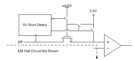
Fig. 4: USB 2.0 High-Speed Receiver Voltage Stress Protection
The USB 2.0 PHY is also required to drive 3.3-V FS/LS waveforms in addition to withstanding a 5-V short condition. Fig. 5 shows a simplified version of the Synopsys DesignWare USB 2.0 PHY transmitter stage that is implemented with 2.5-V thick oxide devices only.
Cascode devices P2 and N2 are used to limit voltages on devices P1 and N1. No two terminals in any transistor ever experience more than 2.75-V of stress across the junctions in any mode of operation, including a 5-V short. Drain/Source to bulk junctions (Vdb, Vsb) are not included as they typically have much higher breakdown voltages i.e. 7-9-V. In a 5-V short condition, the gate of P2 is pulled to 5-V, shutting off the path to vdd33 through P1. P1 and N1 are both turned off in this state. The predrivers provide 2.5-V swing signals to P1 and N1 and ensure the gate oxides are not overstressed.
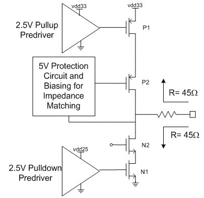
Fig. 5: Synopsys DesignWare USB 2.0 PHY FS/LS Driver Circuit
Device junction stress is checked in all modes of operation and short conditions. The BIASCHK feature in HSPICE checks all junctions for stress exceeding certain limits during functional transient simulations. The flow checks the voltage across all device junctions (Vgd, Vgs, Vds, Vgb) and flags any levels that exceed specified limits. The result is a report that summarizes stressed devices, if any, and the extent and duration for which they exceeded the limits. These results are then used to modify the design to guarantee “stress free†operation.
B. HCI and NBTI
Negative Temperature Bias Instability (NBTI) and Hot Carrier Injection (HCI) are becoming a major concern in predicting long-term MSIP performance. NBTI occurs under negative gate voltages and degrades the device drive current and is typically modeled as a shift in Vt of the degraded device. NBTI predominantly affects the PMOS device, and like HCI, the degradation accelerates at high temperatures. HCI occurs when a short channel device experiences a large lateral electric field across the drain-source junction and predominantly affects NMOS devices. Device degradation and threshold shifts result from impact ionization as carriers are injected into the gate oxide. HCI is typically modeled as a reduction in drive strength or Idsat shift.
Design techniques can be used to minimize the impact on circuit performance associated with HCI and NBTI degradation. The Synopsys DesignWare USB 2.0 PHY design implements NBTI/HCI protection circuitry throughout the PHY to help mitigate device and circuit degradation. An example of a USB 2.0 high speed receive path is shown in Fig. 6. The circuit is typically designed with PMOS input stages in order to handle the low common mode voltage in high speed mode (200mV). As a result, these circuits are susceptible to NBTI induced degradation which can ultimately compromise compliance by causing large input offset voltages in these circuits. To eliminate any NBTI induced offsets, the inputs are pulled to the same voltage during suspend mode, thus introducing symmetric stress on both inputs to the differential pair thereby reducing the induced offset.
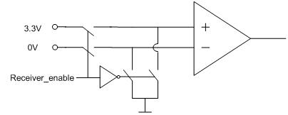
Fig. 6: Inputs to PMOS diff pair are pulled to common voltage in suspend mode.
The voltage regulator in Fig. 1 has a thick oxide NMOS source follower that sustains a large voltage across its drain-source junction. The NMOS experiences HCI degradation, but because it’s in a feedback loop, the degradation is compensated by feedback. In addition, non-minimum length devices are used to increase the lifetime of the device. As shown in the following equation, the lifetime of the device is strongly dependent on the gate length since a >> 1. [Wong, 1996]
 (3)
(3)
C. HSPICE Device Degradation Simulations
Despite the design techniques employed, device degradation cannot be entirely avoided; in some cases, it is difficult to detect via circuit inspection. Devices degrade over time even at nominal temperature and voltages. The design of highly reliable circuits must include simulating the long term effects of HCI and NBTI degradation to verify circuit performance over the lifetime of the IP. Critical circuit parameters such as jitter, skew, offset and duty cycle can be affected and if long term performance is not verified—can easily fall out-of-specification over time.
The degradation of the threshold voltage shift (due to NBTI) and Idsat shift (due to HCI) must be incorporated into circuit simulations in order to properly verify the MSIP. The degradation parameter is based on the numerical solution for the reaction-diffusion mechanism, which is a general model applicable to various reliability effects such as NBTI, HCI, NCS, and SEE. [Vattikonda, 2007]
The Vt shift and Idsat degradation can be modeled using VerilogA wrappers. Fig. 7 shows a simplified model of an inverter after NBTI and HCI effects are included. The flow requires the circuit to be run twice. The first run calculates the operating conditions, junction voltages, and duty cycles of the waveforms. This information is used to build a degraded circuit. The Vt shift and Idsat degradation is then extrapolated to the end-of-life and modeled using VerilogA wrappers. The circuit is then run a second time to check the circuit performance at the end-of-life.
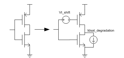
Fig.7: Model of Inverter with NBTI and HCI Effect
Fig. 8 below shows a plot of an inverter output before and after aging (end of life = 100K power on hours).
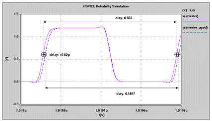
Fig. 8: Inverter Output Before and After Aging
D. Electromigration
Electromigration is the gradual movement of metal atoms due to the momentum transfer between conducting electrons and the metal. Electromigration reduces the reliability of the IC, because over time a failure in the interconnect can occur. As metal stacks continue to get thinner and the current handling capability of the thin metal stacks decreases, satisfying EM constraints is becoming more difficult for designs at 65-nm and smaller.
HSIM Reliability Analysis is used to simulate EM in both power and signal nets under various operating conditions. The simulation highlight nets in the layout with different colors depending on how close the current densities are relative to the process limits. The simulator enables you to quickly identify areas where EM can be a problem and to make necessary layout updates. For example, Fig. 9 shows a predriver stage that has electromigration violations highlighted in red.
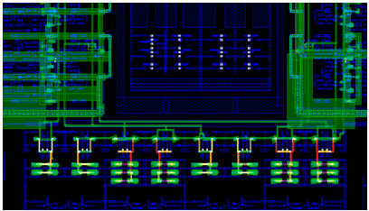
Fig. 9: Electromigration plotted onto GDS layout.
In summary, the Synopsys MSIP reliability flow shown in Fig. 10 consists of three main analyses. Junction stress, device reliability, and electromigration analysis are all built into the flow to ensure long-term design reliability.
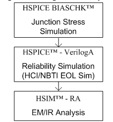
Fig. 10: Synopsys IP Reliability Flow
IV. Design for Yield
Yield is another major factor for quality IP. The major cause of low yield can often be attributed to parametric shifts caused by circuit offsets. These offsets are normally a result of circuit and device mismatch. The mismatch can be divided into two groups: systematic mismatch and random mismatch. Random mismatches are caused by processing effects such as doping non-uniformity, and they affect each device differently and in a random order. Systematic mismatch is caused by effects such as Shallow Trench Isolation Stress (STI), Well Proximity Effect (WPE), asymmetric layout and model inaccuracy. The following section focuses on how to design and lay out MSIP so that the effects of these mismatches are reduced and/or predicted. The concept of analog programmability is also introduced, which helps to reduce the impact of inaccurate modeling—especially when IP is developed early on in the process development cycle.
A. Random Mismatch
Mismatch in device characteristics caused by manufacturing variations exists in every circuit. In these cases, the mismatch can only be truly understood by extensive circuit analysis and extensive Monte Carlo simulations. While in general, random mismatch is inversely proportional to the devices’ dimensions it also depends on the circuit itself and the parameter for which the variation is to be minimized.
For example, the current mismatch of the simple current mirror, shown in Fig. 11, can be expressed in the following equation:
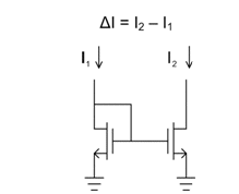
Fig. 11: Current Mirror Mismatch
 (4)
(4)
Where,
 (5)
(5)
Therefore, for a given area (W * L), mismatch is minimized by increasing the length (L) of the devices. Obviously, the optimal matching comes at reduced headroom of the current mirror. However, better matching does not always mean a larger L. Monte Carlo simulation is often used to determine the optimal dimension of the devices, especially when complex circuits are involved.
B. Systematic Mismatch
A lot of prominent systematic variations such as STI are related to the physical dimension of the device in deep submicron design. STI is a mechanical stress phenomenon causing systematic variation in device mobility and threshold voltage. The variation is a function of spacing between the edge of the diffusion and the gate and affects PMOS and NMOS differently.
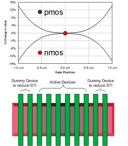
Fig. 12: Layout to reduce STI
There are some layout approaches that are used to reduce the effect of the STI. Fig. 12 shows one such technique by adding dummy devices on the outside of the active devices. This reduces the stress seen by the active device in the middle of the diffusion and thus reduces the Idsat variation in the active devices.
WPE is another major source of device dimension-sensitive systematic variation. Due to the scattering of dopant (N-type and P-type) ions during the implant stage, the devices located near the edge of photo-resist have a different dopant density, and therefore, a different threshold voltage than devices placed further away from the edge.
These systematic mismatches are difficult to predict with schematic-based simulation, because they lack accurate geometry information. To properly verify MSIP final design data should be based on the simulation with a layout extracted netlist that includes well proximity and STI effects. The final result of this extensive simulation flow is a clear picture of the IP’s performance over PVT including random/systematic variation effects.
C. Analog Programmability
Designing MSIP in 65-nm or smaller geometries often implies designing with early device models that are subject to change. The device characteristics can often change by 10–20% over the rollout of a new technology. Designing hard IP that cannot accommodate these process shifts often implies rework, respins, and in some cases, re-architecture of the IP. Most IP customers are not willing to accept this cost and risk. The use of analog programmability enables customers to optimize and tweak the IP characteristics through top-level primary inputs (via metal strapping, software, fuses, and so on). If required due to a process change, customers can potentially re-center the design without the need for expensive mask sets and associated schedule delays.
The Synopsys DesignWare USB 2.0 PHY has many top-level analog programmability inputs to adjust and optimize the high speed eye for unexpected process/model shifts. Fig. 13 shows an example of a baseline eye diagram overlaid with some of the analog programmability enabled. The diagram clearly shows how the analog programmability can be used to adjust DC levels, eye opening (pre-emphasis), cross-over, and rise/fall times.
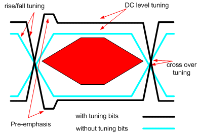
Fig. 13: Eye Diagram With Default Analog Settings
V. Conclusion
Designing high-quality IP in 65-nm technologies requires a comprehensive approach to quality that must include all the key aspects of building quality IP. This paper demonstrated that through the use of novel circuit techniques, power can be reduced significantly—enabling integration in very low-power mobile applications. The paper also presented an intensive reliability verification flow to better predict long-term IP reliability and performance. Lastly this paper introduced the concept of yield optimization and analog programmability, which significantly aids in reducing expensive design respins due to process immaturity.
References
1. Vattikonda R., et al., “A New Simulation Method for NBTI Analysis in SPICE Environment†ISQED 2007, pp. 41 – 46.
2. Bouchakour R., et al. “Modeling and Characterization of the NMOS Transistor Stressed by Hot-Carrier Injection,†ISCAS 1996. pp. 440-443, vol.4.
Synopsys
Abstract
This paper presents some key concepts necessary to design and build high-quality mixed-signal IP in 65‑nm or smaller geometries. The paper addresses design, layout, and verification techniques—with a focus on low-power design, reliability, and yield. Several design examples are presented, highlighting key techniques employed in the Synopsys® DesignWare® Mixed-Signal Intellectual Property (MSIP) portfolio.
I. Introduction
As processes continue to scale aggressively, deep sub-micron, mixed-signal design is becoming more challenging—especially when attempting to produce high-quality mixed-signal intellectual property (MSIP). Stress effects, increased leakage, smaller supply voltages, and reduced oxide thicknesses all make it extremely difficult to build low-power, long-lasting, and high-yielding mixed-signal IP. This paper discusses the three main factors often associated with MSIP: power, reliability, and yield, with a focus on design and verification flows to improve quality. Examples of MSIP includes the USB 2.0 PHY, ADC/DAC, PLL, SERDES (PCI Express®, SATA, XAUI), and DDR.
Section II of this paper presents an overview of some low-power design concepts and provides some examples of low-power circuits from the Synopsys DesignWare MSIP portfolio. This section describes some ultra-low-power techniques used in designs where very aggressive power reduction is necessary to enable integration into mobile applications.
Section III of the paper discusses some key stress effects found in deep sub-micron processes such as Hot Carrier Injection HCI, Negative Bias Temperature Instability (NBTI), and general gate oxide dielectric stress. This section presents design techniques that can be implemented in MSIP to help mitigate the impact on long-term analog circuit performance. This section includes an example of how to build high-voltage tolerant circuits using thinner oxide devices by employing clamping, cascoding, and regulation to reduce gate oxide stress. This section also presents a reliability flow that helps to better predict the MSIP’s long-term performance and reliability. This flow includes automated stress checks, and end-of-life and electro-migration (EM) simulations.
Finally, Section IV outlines some key techniques used to design MSIP with high manufacturability and production-level yield. This section discusses some key sources of mismtach that can ultimately impact yield. The concept of analog programmability is also introduced as a feature for optimizing yield in designs where process shifts require recentering of the design. This analog programmabilty is key to optimizing yield and reducing the need for costly respins.
II. Low-Power Design
Power—one of the most important factors in defining quality MSIP and lowering power consumption—must be considered early in the design phase. The following examples demonstrate several methods and architectures used in MSIP to minimize power—both in active and sleep/low-power modes.
The following is an example of a low-power, high-speed driver used in the Synopsys DesignWare USB 2.0 PHY. Power is kept very low with the use of a voltage-mode driver, shown in Fig.. 1. A voltage-mode driver draws 50% less current from the supply when compared to a conventional current-mode driver shown in Fig.. 2. In fact, for AC-coupled systems such as PCI Express®, SATA, and XAUI, a voltage-mode driver draws 25% of the supply current of a current-mode implementation. For example, a classical USB 2.0 driver requires nominal amplitude of 400 mV for high-speed data transmission into a 45-ohm load. The static power dissipation from the supply for a current-mode driver is:
 (1)
(1)Whereas, the power dissipation from the supply for a voltage-mode driver is:
 (2)
(2)
Fig. 1: Simplified Voltage Mode Driver Implemented in Synopsys DesignWare USB 2.0 PHY

Fig. 2: Conventional USB 2.0 PHY Current-Mode Driver
Another power-reduction technique is shown in the DesignWare USB 2.0 PHY high-speed receive path (Fig. 3). Power is optimized by level shifting down into the low-voltage core device domain as early as possible in the signal path so that its device characteristics are leveraged as much as possible in order to reduce power. This strategy enables most high-frequency analog signal processing to be done in the low-voltage domain (for example, high-speed squelch detection and high speed receive function are implemented using low voltage core devices).

Fig. 3: Synopsys DesignWare USB 2.0 PHY Receiver Front End
Low-power design is also important in sleep modes (non-functional modes) especially for mobile devices. For example, in the USB protocol the PHY can be held in suspend mode for long periods of time. As a result the power dissipation in this mode can become a significant portion of the total and must be scaled aggressively.
Power gating in digital circuits is often used where more aggressive power reduction is necessary. Power gating helps reduce both channel and gate leakage by collapsing the supply and eliminating the leakage current path. This can be implemented on a sub-block level by implementing collapsible, thick-oxide regulators that can be disabled in low-power modes. These regulators are inherently used throughout MSIP design as shown in Fig 1. Digital supply leakage often dominates the power down current and so many SOC's collapse the digital (core) supply rail in these modes as well. Doing so can cause serious side-effects as analog level-shifters found in MSIP can often cause excessive current draw. Special care in the design of level shifters found in MSIP is necessary to avoid this. One example includes circuitry that detects when the digital power supply is collapsed; the circuitry then presets the analog control signals to the IDDQ state thereby eliminating unwanted leakage current.
III. Reliability and Stress Mitigation
In deep sub-micron CMOS, device degradation and stress mitigation are important considerations when producing high-quality IP. Stress mitigation is becoming more complex as circuits mix thick and thin oxide devices in an effort to optimize power, performance, and area. Junction stress, device reliability, and electromigration analysis must be built into the flow to verify the long-term reliability of the design.
A. Stress Mitigation through Design
As CMOS technologies continue to scale, the I/O voltage and its associated thick oxide device have also scaled. Several standards still support 3.3-V signaling while the MSIP is often designed into technologies where the thick oxide devices can only sustain 1.8‑V or 2.5-V junction stress. For example, the USB 2.0 PHY still requires the front-end receive/transmit 3.3‑V signals in FS/LS modes and must tolerate input waveforms from -1 V through 4.6 V. In addition, the transmitters and receivers must be able to handle a short to 5.25 V for extended periods of time. All of these electrical conditons must be tolerated without overstressing the junctions above process limits.
The following example shows some design techniques used to protect the I/O in the Synopsys USB 2.0 PHY with the use of 2.5-V oxide devices only. Fig. 4 shows the simplified receive path. A series NMOS biased at 2.5-V protects the input diff pair from detecting any signals larger than 2.5 – Vt. The circuit is also designed to clamp the input of the receiver to 2.5-V in a 5-V short situation even when no power is supplied. When a 5-V short is detected and when vdd25 is off, a 2.5-V signal is generated from DP and applied to the gate of the NMOS and to the inputs of the receiver.

Fig. 4: USB 2.0 High-Speed Receiver Voltage Stress Protection
The USB 2.0 PHY is also required to drive 3.3-V FS/LS waveforms in addition to withstanding a 5-V short condition. Fig. 5 shows a simplified version of the Synopsys DesignWare USB 2.0 PHY transmitter stage that is implemented with 2.5-V thick oxide devices only.
Cascode devices P2 and N2 are used to limit voltages on devices P1 and N1. No two terminals in any transistor ever experience more than 2.75-V of stress across the junctions in any mode of operation, including a 5-V short. Drain/Source to bulk junctions (Vdb, Vsb) are not included as they typically have much higher breakdown voltages i.e. 7-9-V. In a 5-V short condition, the gate of P2 is pulled to 5-V, shutting off the path to vdd33 through P1. P1 and N1 are both turned off in this state. The predrivers provide 2.5-V swing signals to P1 and N1 and ensure the gate oxides are not overstressed.

Fig. 5: Synopsys DesignWare USB 2.0 PHY FS/LS Driver Circuit
Device junction stress is checked in all modes of operation and short conditions. The BIASCHK feature in HSPICE checks all junctions for stress exceeding certain limits during functional transient simulations. The flow checks the voltage across all device junctions (Vgd, Vgs, Vds, Vgb) and flags any levels that exceed specified limits. The result is a report that summarizes stressed devices, if any, and the extent and duration for which they exceeded the limits. These results are then used to modify the design to guarantee “stress free†operation.
B. HCI and NBTI
Negative Temperature Bias Instability (NBTI) and Hot Carrier Injection (HCI) are becoming a major concern in predicting long-term MSIP performance. NBTI occurs under negative gate voltages and degrades the device drive current and is typically modeled as a shift in Vt of the degraded device. NBTI predominantly affects the PMOS device, and like HCI, the degradation accelerates at high temperatures. HCI occurs when a short channel device experiences a large lateral electric field across the drain-source junction and predominantly affects NMOS devices. Device degradation and threshold shifts result from impact ionization as carriers are injected into the gate oxide. HCI is typically modeled as a reduction in drive strength or Idsat shift.
Design techniques can be used to minimize the impact on circuit performance associated with HCI and NBTI degradation. The Synopsys DesignWare USB 2.0 PHY design implements NBTI/HCI protection circuitry throughout the PHY to help mitigate device and circuit degradation. An example of a USB 2.0 high speed receive path is shown in Fig. 6. The circuit is typically designed with PMOS input stages in order to handle the low common mode voltage in high speed mode (200mV). As a result, these circuits are susceptible to NBTI induced degradation which can ultimately compromise compliance by causing large input offset voltages in these circuits. To eliminate any NBTI induced offsets, the inputs are pulled to the same voltage during suspend mode, thus introducing symmetric stress on both inputs to the differential pair thereby reducing the induced offset.

Fig. 6: Inputs to PMOS diff pair are pulled to common voltage in suspend mode.
The voltage regulator in Fig. 1 has a thick oxide NMOS source follower that sustains a large voltage across its drain-source junction. The NMOS experiences HCI degradation, but because it’s in a feedback loop, the degradation is compensated by feedback. In addition, non-minimum length devices are used to increase the lifetime of the device. As shown in the following equation, the lifetime of the device is strongly dependent on the gate length since a >> 1. [Wong, 1996]
 (3)
(3)C. HSPICE Device Degradation Simulations
Despite the design techniques employed, device degradation cannot be entirely avoided; in some cases, it is difficult to detect via circuit inspection. Devices degrade over time even at nominal temperature and voltages. The design of highly reliable circuits must include simulating the long term effects of HCI and NBTI degradation to verify circuit performance over the lifetime of the IP. Critical circuit parameters such as jitter, skew, offset and duty cycle can be affected and if long term performance is not verified—can easily fall out-of-specification over time.
The degradation of the threshold voltage shift (due to NBTI) and Idsat shift (due to HCI) must be incorporated into circuit simulations in order to properly verify the MSIP. The degradation parameter is based on the numerical solution for the reaction-diffusion mechanism, which is a general model applicable to various reliability effects such as NBTI, HCI, NCS, and SEE. [Vattikonda, 2007]
The Vt shift and Idsat degradation can be modeled using VerilogA wrappers. Fig. 7 shows a simplified model of an inverter after NBTI and HCI effects are included. The flow requires the circuit to be run twice. The first run calculates the operating conditions, junction voltages, and duty cycles of the waveforms. This information is used to build a degraded circuit. The Vt shift and Idsat degradation is then extrapolated to the end-of-life and modeled using VerilogA wrappers. The circuit is then run a second time to check the circuit performance at the end-of-life.

Fig.7: Model of Inverter with NBTI and HCI Effect
Fig. 8 below shows a plot of an inverter output before and after aging (end of life = 100K power on hours).

Fig. 8: Inverter Output Before and After Aging
D. Electromigration
Electromigration is the gradual movement of metal atoms due to the momentum transfer between conducting electrons and the metal. Electromigration reduces the reliability of the IC, because over time a failure in the interconnect can occur. As metal stacks continue to get thinner and the current handling capability of the thin metal stacks decreases, satisfying EM constraints is becoming more difficult for designs at 65-nm and smaller.
HSIM Reliability Analysis is used to simulate EM in both power and signal nets under various operating conditions. The simulation highlight nets in the layout with different colors depending on how close the current densities are relative to the process limits. The simulator enables you to quickly identify areas where EM can be a problem and to make necessary layout updates. For example, Fig. 9 shows a predriver stage that has electromigration violations highlighted in red.

Fig. 9: Electromigration plotted onto GDS layout.
In summary, the Synopsys MSIP reliability flow shown in Fig. 10 consists of three main analyses. Junction stress, device reliability, and electromigration analysis are all built into the flow to ensure long-term design reliability.

Fig. 10: Synopsys IP Reliability Flow
IV. Design for Yield
Yield is another major factor for quality IP. The major cause of low yield can often be attributed to parametric shifts caused by circuit offsets. These offsets are normally a result of circuit and device mismatch. The mismatch can be divided into two groups: systematic mismatch and random mismatch. Random mismatches are caused by processing effects such as doping non-uniformity, and they affect each device differently and in a random order. Systematic mismatch is caused by effects such as Shallow Trench Isolation Stress (STI), Well Proximity Effect (WPE), asymmetric layout and model inaccuracy. The following section focuses on how to design and lay out MSIP so that the effects of these mismatches are reduced and/or predicted. The concept of analog programmability is also introduced, which helps to reduce the impact of inaccurate modeling—especially when IP is developed early on in the process development cycle.
A. Random Mismatch
Mismatch in device characteristics caused by manufacturing variations exists in every circuit. In these cases, the mismatch can only be truly understood by extensive circuit analysis and extensive Monte Carlo simulations. While in general, random mismatch is inversely proportional to the devices’ dimensions it also depends on the circuit itself and the parameter for which the variation is to be minimized.
For example, the current mismatch of the simple current mirror, shown in Fig. 11, can be expressed in the following equation:

Fig. 11: Current Mirror Mismatch
 (4)
(4)Where,
 (5)
(5)Therefore, for a given area (W * L), mismatch is minimized by increasing the length (L) of the devices. Obviously, the optimal matching comes at reduced headroom of the current mirror. However, better matching does not always mean a larger L. Monte Carlo simulation is often used to determine the optimal dimension of the devices, especially when complex circuits are involved.
B. Systematic Mismatch
A lot of prominent systematic variations such as STI are related to the physical dimension of the device in deep submicron design. STI is a mechanical stress phenomenon causing systematic variation in device mobility and threshold voltage. The variation is a function of spacing between the edge of the diffusion and the gate and affects PMOS and NMOS differently.

Fig. 12: Layout to reduce STI
There are some layout approaches that are used to reduce the effect of the STI. Fig. 12 shows one such technique by adding dummy devices on the outside of the active devices. This reduces the stress seen by the active device in the middle of the diffusion and thus reduces the Idsat variation in the active devices.
WPE is another major source of device dimension-sensitive systematic variation. Due to the scattering of dopant (N-type and P-type) ions during the implant stage, the devices located near the edge of photo-resist have a different dopant density, and therefore, a different threshold voltage than devices placed further away from the edge.
These systematic mismatches are difficult to predict with schematic-based simulation, because they lack accurate geometry information. To properly verify MSIP final design data should be based on the simulation with a layout extracted netlist that includes well proximity and STI effects. The final result of this extensive simulation flow is a clear picture of the IP’s performance over PVT including random/systematic variation effects.
C. Analog Programmability
Designing MSIP in 65-nm or smaller geometries often implies designing with early device models that are subject to change. The device characteristics can often change by 10–20% over the rollout of a new technology. Designing hard IP that cannot accommodate these process shifts often implies rework, respins, and in some cases, re-architecture of the IP. Most IP customers are not willing to accept this cost and risk. The use of analog programmability enables customers to optimize and tweak the IP characteristics through top-level primary inputs (via metal strapping, software, fuses, and so on). If required due to a process change, customers can potentially re-center the design without the need for expensive mask sets and associated schedule delays.
The Synopsys DesignWare USB 2.0 PHY has many top-level analog programmability inputs to adjust and optimize the high speed eye for unexpected process/model shifts. Fig. 13 shows an example of a baseline eye diagram overlaid with some of the analog programmability enabled. The diagram clearly shows how the analog programmability can be used to adjust DC levels, eye opening (pre-emphasis), cross-over, and rise/fall times.

Fig. 13: Eye Diagram With Default Analog Settings
V. Conclusion
Designing high-quality IP in 65-nm technologies requires a comprehensive approach to quality that must include all the key aspects of building quality IP. This paper demonstrated that through the use of novel circuit techniques, power can be reduced significantly—enabling integration in very low-power mobile applications. The paper also presented an intensive reliability verification flow to better predict long-term IP reliability and performance. Lastly this paper introduced the concept of yield optimization and analog programmability, which significantly aids in reducing expensive design respins due to process immaturity.
References
1. Vattikonda R., et al., “A New Simulation Method for NBTI Analysis in SPICE Environment†ISQED 2007, pp. 41 – 46.
2. Bouchakour R., et al. “Modeling and Characterization of the NMOS Transistor Stressed by Hot-Carrier Injection,†ISCAS 1996. pp. 440-443, vol.4.
