Yoav Lavi, VLSI Plus
Raanana, Israel
Abstract
A two data-lane Serial Video Receiver (SVR), compatible with both MIPI CSI2 and SMIA CCP2 standards, with speeds of up to 2Gbps, is presented.
The IP comprises an analog-domain hard-core PHY layer, a PHY-Extension unit (PHYEX) which extends the analog functions to cover MIPI full PHY requirements, and a PHY Protocol Interface unit (PPI), which merges lanes, detects and corrects errors and translates the various video formats to pixels.
An elaborate interrupt mechanism is included, for normal operation as well as for a multitude of error conditions. For error-free operation, a minimum of CPU handling is required, and in a typical system the SVR outputs pixels into an off-IP rate-match FIFO.
The SVR IP comprises some 14,000 gates. It was implemented in standard 90nm CMOS technology, as well as in 80nm.
Cellular Video Interface goes Serial
As cell-phone cameras get into the multi-mega pixel densities, parallel communication between the imager and the application processor is a source of noise, with typically 11 or 13 single-ended lines toggling at ever increasing frequencies.
The solution, as outlined by industry leaders, is to use balanced and fully matched differential lines for the transmission. With well designed differential conductors, the emitted noise due to line imperfections is small, allowing the serialization of the pixel stream.
The wire pairs carrying differential data will be referred to as Lanes in the remainder of this document.
Several standardization efforts have been in progress in recent years. Two of them are supported by the SVR, and discussed in the present paper – SMIA CCP2 and MIPI D-PHY / CSI2.
SMIA CCP2
SMIA (Standard Mobile Imaging Architecture) defines, among others, the serial interface between the camera and the Application Processor, comprising a slow control interface [1] and a fast pixel-transfer interface (CCP2).
Pixel transfer media is two SUB-LVDS differential pairs, connecting the transmitter (image sensor) to the receiver (typically an application processor). The two pairs can be data/clock, where the data lane is sampled on clock lane transitions, or data/strobe, where the sampling clock is derived by an exclusive-or function of the data and strobe lanes, and thus the maximum toggling frequency for either lane is ½ the data rate.
The CCP2 defines three classes:
MIPI D-PHY / CSI2
MIPI (Mobile Industry Processor Interface) defines a set of standards for serial interface between mobile processor units. The underlying physical layer is defined in the D-PHY standard (which is planned to be replaced by the M-PHY standard). The protocol standard for camera initiated transmissions is CSI2.
The D-PHY / CSI standards specify one DDR clock lane, and from one to four data lanes. In addition to high speed differential signaling, low-power CMOS signaling is also defined using the same wires, allowing the interface to assume low power when no data is transmitted, and to transmit control information at low speed.
MIPI CSI supports short packets, used for synchronization and for event signaling, and long packets, typically used to transfer video lines.
Key CCP2 and CSI / D-PHY Features
The following table lists some of the key features of both standards:
Notes:
(1) – Maximum rate is not defined in the MIPI D-PHY / CSI standard; the value of 1Gbps per data lane is an expected practical limit.
(2) – While other formats are defined in the CCP2 standard, they are not supported by SMIA
VLSI Plus SVR
VLSI Plus SVR is an IP core implementing the receiver side of both SMIA CCP2 and MIPI CSI2, supporting 650Mbps in SMIA mode and up to 2Gbps in two data-lane MIPI mode. The SVR is targeted at manufacturers of application processors and baseband chips for the wireless market.
The main guideline for the SVR definition was – allowing minimum or no host intervention for normal error-free operation, while providing all needed data in case errors are detected.
Thus, the SVR delivers a pixel stream after error detection and correction, and after video format conversion. Output pixels are typically stored in an off-IP FIFO, which is read by off-IP video processing hardware or software.
A typical system connection of the SVR is depicted in Figure 1. The clock lane and one or two data lanes which originate in the image sensor are connected to the chip external pins. The PHY level processing of the incoming packets is done by an analog front end, and by a digital PHY-Extension unit (PHYEX). The combined analog and PHY-Extension processing covers the PHY functionality as defined in the MIPI D-PHY standard. This will be elaborated on below.
Protocol level processing is done at the PPI (PHY Protocol Interface) unit, which is configured by a host CPU through an AMBA APB bus. If errors are detected, the SVR asserts the Interrupt line; the CPU can then check for the error source, and, if possible, continue. In addition, the SVR can be programmed to alert the CPU whenever a packet is received.
The PPI outputs a reconstructed pixel stream, using the 24 bit pixel-out bus, along with a pixel-valid line. The output pixel stream is typically stored in a rate-matching FIFO (not part of the SVR) for video processing by software and/or hardware.
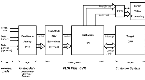
Figure 1: System Connection of VLSI Plus SVR
Extended PHY Concept
MIPI D-PHY standard defines a plurality of tasks which should be executed at the PHY level. Those include:
In addition, the PHY operation must adhere with tight timing parameters, some of which specified in terms of UI – the reconstructed transmission clock period, others specified in absolute time units (i.e. seconds), and yet others in a combination of UI units and absolute time units.
Due to the high speed involved and the differential nature of the protocol, at least some of the PHY design should be done in an analog-signal design paradigm. On the other hand, the complexity of the required D-PHY tasks is relatively high, deeming a fully analog design inefficient.
The solution chosen by VLSI Plus is separation of the PHY implementation to two parts – one which handles the high speed and the differential receiver part, and one which works in a digital domain, using standard ASIC methodology. The analog part is process-specific; it can be obtained from VLSI Plus partners, or can be built by the customer, according to specifications provided by VLSI Plus.
The digital part is referred to as PHYEX, or PHY Extension unit. It is provided by VLSI Plus as part of the SVR deliverable, or can be acquired separately.
The concept of an analog PHY and a PHY Extension (PHYEX) unit is depicted in Figure 2.
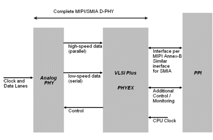
Figure 2: PHYEX Concept
The analog PHY outputs the CMOS level state of the incoming lanes, as well as the de-serialized data, in 8-bit units. It is controlled by parallel lines, indicating if the termination should be connected or not, the high-speed receiver should be on or off, and others.
The PHYEX is also the place where incoming data, ticked by the transmitted clock, is synchronized to the CPU clock, which also serves as the main SVR clock.
The interface signals from the PHYEX to the PPI are defined in an annex to the MIPI D-PHY standard. Those same signals are also used when the SVR is in SMIA mode.
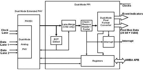
Figure 3: SVR Block Diagram
SVR Block Diagram
Figure 3 depicts the block diagram of VLSI Plus SVR. The PHY, comprising an analog PHY and the PHYEX, outputs aligned data, in one or two bytes, to the PPI. End of Transmission is detected according to state machines in the PHYEX. The two lanes are then merged in the PPI to a single byte stream, which is forwarded to header/footer handling.
The header/footer handler corrects the header according to the embedded ECC code (in CSI mode). In addition it encodes the header to extract the type of packet being received. It can also get the number of bytes expected in the current packet, so it would know when the packet is expected to end. Lastly, the header/footer handler keeps track of the packet CRC, and will signal interrupt if it is not clear when the packet ends.
Other monitored error conditions include mismatches between start and end of packet, time-out at various levels, illegal state at the PHYEX state machines, and more.
MIPI CSI standard supports 18 pixel formats, in addition to user defined formats, as well as predefined and user defined short packets. The standard defines bit packing of pixels for reduced bandwidth. The packing is relatively complex; for example, 8 seven-bit RAW7 pixels are bit-packed
to fill 7 consecutive bytes, and, for another example, 4 RAW10 pixels are packed to fill 5 bytes, when bits [9:2] of the four pixels are transmitted first, followed by an assembly of the LS bits [1:0] of the four pixels, packed in a single byte.
While other CSI receivers rely on the CPU to reconstruct the pixels from the transmitted bytes, VLSI Plus SVR is equipped to decode all video formats in hardware, and output the original pixels to the host.
Self Calibration
In order to support the timing parameters defined by MIPI D-PHY standard, which are sometimes expressed in terms of the transmitter clock frequency (UI), the SVR is equipped with a self-calibration unit. This unit measures the ratio between the transmitter clock frequency and the SVR main clock. The measured ratio is stored in a register, which is then used in order to generate the specified timing intervals. The underlying assumption is that the transmitter frequency (as well as the SVR frequency) remains substantially constant. If it changes, recalibration is needed, initiated by the host CPU.
Beyond the Standards – Relaxed Skew Requirements
VLSI Plus SVR exceeds the requirements of both MIPI CSI2/D-PHY and SMIA CCP2 requirements in several aspects.
Both SMIA CCP2 and MIPI CSI2 assume tight phase relationship between the clock and the data lanes. For example, with 1Gbps per lane operation, the skew between the clock lane and each of the data lanes, which is accumulated in the interconnect, should not exceed ±200ps.
However, it is very likely that when the standards are widely accepted and implemented in a plethora of phone models, including very low cost ones, this requirement may be hard to meet; especially when the wiring from the camera to the main phone board may have to go through hinges and connectors.
Our SVR, therefore, allows for the addition of a programmable delay between the clock and data lanes. With this feature, a fixed skew of practically any value can be tolerated by the SVR, in both MIPI and SMIA modes.
Beyond the Standards – Better CCP end-of-packet Detection
In MIPI CSI2, the number of bytes in each packet is specified in the packet header. The receiver counts the received bytes, and when the last byte has been received, it checks the CRC and signals end-of-packet.
In SMIA CCP2, end of packet is signaled by a synchronization code. The receiver looks for this code, throughout the packet.
However, if, as a result of noise, the end-of-packet synchronization code is corrupted and hence missed by the receiver, it will not be detected until the next packet. When the next packet starts, the receiver will get a start-of-packet sync code while it is expecting end-of-packet sync code; an error will be detected, but it will be impossible for the receiver to tell if the error refers to a missing end-of-packet for the previous packet, or to a wrong sync code for the current packet. The result would be - loss of two packets rather than one.
In VLSI Plus SVR, as a mechanism to count transmission bytes is already in place for the CSI mode, this counter can be used to help detect end-of packet in SMIA mode. The user has the option to program the number-of-bytes register, and the SVR will count the received bytes, and tell that a packet end is missing before the sync of the next packet is received. Thus, only a single packet will be lost.
Beyond the Standards – Additional CCP Formats
While the SMIA standard supports only two video formats – RAW8 and RAW10, other formats are defined in the CCP specifications. The SVR currently implements, in addition to SMIA RAW8 and RAW10, also RAW12. Other formats, including the full CSI2 scope, can be easily added, per customer request.
Performance
The SVR has been implemented in standard 90nm CMOS technology, as well as in 80nm. The performance, in terms of transmission rate, is determined by the slowest of the three following units: the analog front end, where data rate is measured in bits-per-second, the byte-oriented digital processing, where data rate is measured in bytes-per-second, and the digital pixel-handling part, where rate is measured in pixels per second. The analog front end is designed to support 1Gbps per data lane. For the digital part, clock frequency should be chosen according to the required data rate [2]. The following table depicts some performance numbers for the SVR, assuming a clock frequency of 275MHZ. The table shows performance rates in pixel-per-second and bits per second, for single lane and dual lane configuration, CSI mode.
Summary and Customization
The SVR supports two standards (MIPI and SMIA), with three classes in SMIA, and one or two data lanes in MIPI. All MIPI video formats are supported, as well as an extensive error reporting mechanism, and 21 control AMBA registers, some of them occupying full 32 bits. This rich functionality is implemented in some 14,000 gates, not including the analog PHY but including all internal memories (which are implemented as registers).
The SVR is built in a flexible manner, allowing easy customization to customers’ needs. In particular, the size of the IP can be considerably reduced if the customer does not need some of the features. CCP2-only implementation, for example, consumes about a third of the gates, and can be implemented using standard analog components for the front end.
To take another example, if a single data lane is needed, large portions of the digital as well as the analog PHY could be saved. And, as a third example if the only formats to be considered are RAW, a lot of the video format conversion hardware will be spared.
VLSI Plus can do those and other customization tasks, at a relatively short time frame.
[1] The slow control interface, common also to the MIPI standard, is typically supported by an I2C interface, and will not be discussed in this paper
[2] The selection of this frequency also determines the accuracy of some of the timing parameters.
Raanana, Israel
Abstract
A two data-lane Serial Video Receiver (SVR), compatible with both MIPI CSI2 and SMIA CCP2 standards, with speeds of up to 2Gbps, is presented.
The IP comprises an analog-domain hard-core PHY layer, a PHY-Extension unit (PHYEX) which extends the analog functions to cover MIPI full PHY requirements, and a PHY Protocol Interface unit (PPI), which merges lanes, detects and corrects errors and translates the various video formats to pixels.
An elaborate interrupt mechanism is included, for normal operation as well as for a multitude of error conditions. For error-free operation, a minimum of CPU handling is required, and in a typical system the SVR outputs pixels into an off-IP rate-match FIFO.
The SVR IP comprises some 14,000 gates. It was implemented in standard 90nm CMOS technology, as well as in 80nm.
Cellular Video Interface goes Serial
As cell-phone cameras get into the multi-mega pixel densities, parallel communication between the imager and the application processor is a source of noise, with typically 11 or 13 single-ended lines toggling at ever increasing frequencies.
The solution, as outlined by industry leaders, is to use balanced and fully matched differential lines for the transmission. With well designed differential conductors, the emitted noise due to line imperfections is small, allowing the serialization of the pixel stream.
The wire pairs carrying differential data will be referred to as Lanes in the remainder of this document.
Several standardization efforts have been in progress in recent years. Two of them are supported by the SVR, and discussed in the present paper – SMIA CCP2 and MIPI D-PHY / CSI2.
SMIA CCP2
SMIA (Standard Mobile Imaging Architecture) defines, among others, the serial interface between the camera and the Application Processor, comprising a slow control interface [1] and a fast pixel-transfer interface (CCP2).
Pixel transfer media is two SUB-LVDS differential pairs, connecting the transmitter (image sensor) to the receiver (typically an application processor). The two pairs can be data/clock, where the data lane is sampled on clock lane transitions, or data/strobe, where the sampling clock is derived by an exclusive-or function of the data and strobe lanes, and thus the maximum toggling frequency for either lane is ½ the data rate.
The CCP2 defines three classes:
| Class | Sustained Rate | Signaling |
| 1 | <208Mbps | Data/Clock |
| 2 | 208Mbps-416Mbps | Data/Strobe |
| 3 | 416Mbps-650Mbps | Data/Strobe |
MIPI D-PHY / CSI2
MIPI (Mobile Industry Processor Interface) defines a set of standards for serial interface between mobile processor units. The underlying physical layer is defined in the D-PHY standard (which is planned to be replaced by the M-PHY standard). The protocol standard for camera initiated transmissions is CSI2.
The D-PHY / CSI standards specify one DDR clock lane, and from one to four data lanes. In addition to high speed differential signaling, low-power CMOS signaling is also defined using the same wires, allowing the interface to assume low power when no data is transmitted, and to transmit control information at low speed.
MIPI CSI supports short packets, used for synchronization and for event signaling, and long packets, typically used to transfer video lines.
Key CCP2 and CSI / D-PHY Features
The following table lists some of the key features of both standards:
| Feature | CCP2 | D-PHY+CSI2 |
| Lanes | 1 Clock + 1 Data | 1 Clock + 1 to 4 Data |
| Maximum Rate | 650Mbps | 1Gbps per data lane1 |
| Levels | Differential (Sub-LVDS) | Differential (non-standard levels), and unipolar CMOS levels |
| Channels | 8 | 4 |
| Frame Start signaling | Embedded sync code | Short-Packet |
| Line Start Signaling | Embedded sync code | Header info; Optional short packet |
| Frame End Signaling | Embedded sync code | Short Packet |
| Line End Signaling | Embedded sync code | Signal level, packet byte count, optional short packet |
| Illegal pixels | defined, to avoid false sync | Not needed (all values are legal) |
| Header ECC | No | Yes |
| Packet CRC | Yes | Yes |
| Video Formats | RAW8, RAW102 | 18 formats |
| Video Format Specification | Preprogrammed | Specified in the header for each packet |
| Video Compression | Defined | Not defined |
| Short packets | No | Yes |
| CMOS signaling | No | Yes |
| Complexity | Lower | Higher |
Notes:
(1) – Maximum rate is not defined in the MIPI D-PHY / CSI standard; the value of 1Gbps per data lane is an expected practical limit.
(2) – While other formats are defined in the CCP2 standard, they are not supported by SMIA
VLSI Plus SVR
VLSI Plus SVR is an IP core implementing the receiver side of both SMIA CCP2 and MIPI CSI2, supporting 650Mbps in SMIA mode and up to 2Gbps in two data-lane MIPI mode. The SVR is targeted at manufacturers of application processors and baseband chips for the wireless market.
The main guideline for the SVR definition was – allowing minimum or no host intervention for normal error-free operation, while providing all needed data in case errors are detected.
Thus, the SVR delivers a pixel stream after error detection and correction, and after video format conversion. Output pixels are typically stored in an off-IP FIFO, which is read by off-IP video processing hardware or software.
A typical system connection of the SVR is depicted in Figure 1. The clock lane and one or two data lanes which originate in the image sensor are connected to the chip external pins. The PHY level processing of the incoming packets is done by an analog front end, and by a digital PHY-Extension unit (PHYEX). The combined analog and PHY-Extension processing covers the PHY functionality as defined in the MIPI D-PHY standard. This will be elaborated on below.
Protocol level processing is done at the PPI (PHY Protocol Interface) unit, which is configured by a host CPU through an AMBA APB bus. If errors are detected, the SVR asserts the Interrupt line; the CPU can then check for the error source, and, if possible, continue. In addition, the SVR can be programmed to alert the CPU whenever a packet is received.
The PPI outputs a reconstructed pixel stream, using the 24 bit pixel-out bus, along with a pixel-valid line. The output pixel stream is typically stored in a rate-matching FIFO (not part of the SVR) for video processing by software and/or hardware.

Figure 1: System Connection of VLSI Plus SVR
Extended PHY Concept
MIPI D-PHY standard defines a plurality of tasks which should be executed at the PHY level. Those include:
- Reconstruction of the transmitter clock
- Keeping track of Transmission state
- Detecting Error Conditions
- Handling CMOS level signaling
- Escape Mode signaling
- Synchronization to start-of-data, allowing for single-bit errors in the received synch code
- Timely connection and disconnection of the Termination
- Detecting loss of Transmission Clock
- De-serializing the bit-serial pixel stream
In addition, the PHY operation must adhere with tight timing parameters, some of which specified in terms of UI – the reconstructed transmission clock period, others specified in absolute time units (i.e. seconds), and yet others in a combination of UI units and absolute time units.
Due to the high speed involved and the differential nature of the protocol, at least some of the PHY design should be done in an analog-signal design paradigm. On the other hand, the complexity of the required D-PHY tasks is relatively high, deeming a fully analog design inefficient.
The solution chosen by VLSI Plus is separation of the PHY implementation to two parts – one which handles the high speed and the differential receiver part, and one which works in a digital domain, using standard ASIC methodology. The analog part is process-specific; it can be obtained from VLSI Plus partners, or can be built by the customer, according to specifications provided by VLSI Plus.
The digital part is referred to as PHYEX, or PHY Extension unit. It is provided by VLSI Plus as part of the SVR deliverable, or can be acquired separately.
The concept of an analog PHY and a PHY Extension (PHYEX) unit is depicted in Figure 2.

Figure 2: PHYEX Concept
The analog PHY outputs the CMOS level state of the incoming lanes, as well as the de-serialized data, in 8-bit units. It is controlled by parallel lines, indicating if the termination should be connected or not, the high-speed receiver should be on or off, and others.
The PHYEX is also the place where incoming data, ticked by the transmitted clock, is synchronized to the CPU clock, which also serves as the main SVR clock.
The interface signals from the PHYEX to the PPI are defined in an annex to the MIPI D-PHY standard. Those same signals are also used when the SVR is in SMIA mode.

Figure 3: SVR Block Diagram
SVR Block Diagram
Figure 3 depicts the block diagram of VLSI Plus SVR. The PHY, comprising an analog PHY and the PHYEX, outputs aligned data, in one or two bytes, to the PPI. End of Transmission is detected according to state machines in the PHYEX. The two lanes are then merged in the PPI to a single byte stream, which is forwarded to header/footer handling.
The header/footer handler corrects the header according to the embedded ECC code (in CSI mode). In addition it encodes the header to extract the type of packet being received. It can also get the number of bytes expected in the current packet, so it would know when the packet is expected to end. Lastly, the header/footer handler keeps track of the packet CRC, and will signal interrupt if it is not clear when the packet ends.
Other monitored error conditions include mismatches between start and end of packet, time-out at various levels, illegal state at the PHYEX state machines, and more.
MIPI CSI standard supports 18 pixel formats, in addition to user defined formats, as well as predefined and user defined short packets. The standard defines bit packing of pixels for reduced bandwidth. The packing is relatively complex; for example, 8 seven-bit RAW7 pixels are bit-packed
to fill 7 consecutive bytes, and, for another example, 4 RAW10 pixels are packed to fill 5 bytes, when bits [9:2] of the four pixels are transmitted first, followed by an assembly of the LS bits [1:0] of the four pixels, packed in a single byte.
While other CSI receivers rely on the CPU to reconstruct the pixels from the transmitted bytes, VLSI Plus SVR is equipped to decode all video formats in hardware, and output the original pixels to the host.
Self Calibration
In order to support the timing parameters defined by MIPI D-PHY standard, which are sometimes expressed in terms of the transmitter clock frequency (UI), the SVR is equipped with a self-calibration unit. This unit measures the ratio between the transmitter clock frequency and the SVR main clock. The measured ratio is stored in a register, which is then used in order to generate the specified timing intervals. The underlying assumption is that the transmitter frequency (as well as the SVR frequency) remains substantially constant. If it changes, recalibration is needed, initiated by the host CPU.
Beyond the Standards – Relaxed Skew Requirements
VLSI Plus SVR exceeds the requirements of both MIPI CSI2/D-PHY and SMIA CCP2 requirements in several aspects.
Both SMIA CCP2 and MIPI CSI2 assume tight phase relationship between the clock and the data lanes. For example, with 1Gbps per lane operation, the skew between the clock lane and each of the data lanes, which is accumulated in the interconnect, should not exceed ±200ps.
However, it is very likely that when the standards are widely accepted and implemented in a plethora of phone models, including very low cost ones, this requirement may be hard to meet; especially when the wiring from the camera to the main phone board may have to go through hinges and connectors.
Our SVR, therefore, allows for the addition of a programmable delay between the clock and data lanes. With this feature, a fixed skew of practically any value can be tolerated by the SVR, in both MIPI and SMIA modes.
Beyond the Standards – Better CCP end-of-packet Detection
In MIPI CSI2, the number of bytes in each packet is specified in the packet header. The receiver counts the received bytes, and when the last byte has been received, it checks the CRC and signals end-of-packet.
In SMIA CCP2, end of packet is signaled by a synchronization code. The receiver looks for this code, throughout the packet.
However, if, as a result of noise, the end-of-packet synchronization code is corrupted and hence missed by the receiver, it will not be detected until the next packet. When the next packet starts, the receiver will get a start-of-packet sync code while it is expecting end-of-packet sync code; an error will be detected, but it will be impossible for the receiver to tell if the error refers to a missing end-of-packet for the previous packet, or to a wrong sync code for the current packet. The result would be - loss of two packets rather than one.
In VLSI Plus SVR, as a mechanism to count transmission bytes is already in place for the CSI mode, this counter can be used to help detect end-of packet in SMIA mode. The user has the option to program the number-of-bytes register, and the SVR will count the received bytes, and tell that a packet end is missing before the sync of the next packet is received. Thus, only a single packet will be lost.
Beyond the Standards – Additional CCP Formats
While the SMIA standard supports only two video formats – RAW8 and RAW10, other formats are defined in the CCP specifications. The SVR currently implements, in addition to SMIA RAW8 and RAW10, also RAW12. Other formats, including the full CSI2 scope, can be easily added, per customer request.
Performance
The SVR has been implemented in standard 90nm CMOS technology, as well as in 80nm. The performance, in terms of transmission rate, is determined by the slowest of the three following units: the analog front end, where data rate is measured in bits-per-second, the byte-oriented digital processing, where data rate is measured in bytes-per-second, and the digital pixel-handling part, where rate is measured in pixels per second. The analog front end is designed to support 1Gbps per data lane. For the digital part, clock frequency should be chosen according to the required data rate [2]. The following table depicts some performance numbers for the SVR, assuming a clock frequency of 275MHZ. The table shows performance rates in pixel-per-second and bits per second, for single lane and dual lane configuration, CSI mode.
| Format | Performance, PPS | Performance, BPS | ||
| 1 Data lane | 2 Data lanes | 1 Data lane | 2 Data lanes | |
| RAW8 | 125M | 248M | 1000M | 1980M |
| RAW12 | 83M | 165M | 1000M | 1980M |
| RAW6 | 167M | 248M | 1000M | 1732M |
| RGB888 | 42M | 83M | 1000M | 1980M |
| YUV42210b | 100M | 198M | 1000M | 1980M |
Summary and Customization
The SVR supports two standards (MIPI and SMIA), with three classes in SMIA, and one or two data lanes in MIPI. All MIPI video formats are supported, as well as an extensive error reporting mechanism, and 21 control AMBA registers, some of them occupying full 32 bits. This rich functionality is implemented in some 14,000 gates, not including the analog PHY but including all internal memories (which are implemented as registers).
The SVR is built in a flexible manner, allowing easy customization to customers’ needs. In particular, the size of the IP can be considerably reduced if the customer does not need some of the features. CCP2-only implementation, for example, consumes about a third of the gates, and can be implemented using standard analog components for the front end.
To take another example, if a single data lane is needed, large portions of the digital as well as the analog PHY could be saved. And, as a third example if the only formats to be considered are RAW, a lot of the video format conversion hardware will be spared.
VLSI Plus can do those and other customization tasks, at a relatively short time frame.
[1] The slow control interface, common also to the MIPI standard, is typically supported by an I2C interface, and will not be discussed in this paper
[2] The selection of this frequency also determines the accuracy of some of the timing parameters.
