A. Ben Atitallah (1,2), P. Kadionik (2), N. Masmoudi (1), H. Levi (2)
(1) Laboratory of Electronics and Information Technology, Tunisia
(2) IMS laboratory - ENSEIRB , France
Abstract:
This paper presents a dedicated hardware platform for a fast video and image data processing to real time application. The platform supports simultaneous HW/SW codesign and partitioning and based on the FPGA technologies and on a RISC processor. This reduces application design cycle. As an example, the H.263 video encoder is presented
1. Introduction
The necessity for real-time video processing capabilities in embedded systems is generally increasing with time. Real-time video processing is a very data intensive task when compared to many of the normal tasks performed by embedded systems. Even in simple real-time video operations where the algorithmic complexity of the processing is very low, the mere transfer of image data may consume significant system resources.
FPGAs provide an efficient alternative for implementing video processing applications. Modern FPGAs include many attractive characteristics such as: flexibility, low cost, high integration, embedded distributed memories and extensive parallelism. The main purpose of the paper is to practice of the HW/SW codesign process in FPGA. An efficient HW/SW codesign process is the key to design real-time embedded video system application.
This paper is organized as follow. Section 2 describes the embedded video system, the camera and VGA hardware interfaces. The implementation of the HW/SW codesign H.263 video encoder is presented then in section 3. The experiment results are presented in section 4. Section 5 concludes the paper.
2. Embedded Video System
In our video and image processing application, the chain contains acquisition module, processing and restitution of a video signal coming from the video source. The global processing video system is based on a System on Programmable Chip (SoPC): all system components are put into a single chip (FPGA). The synoptic diagram of the realized system is presented in Figure.1.
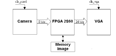
Figure. 1. Video System
For the main processing stage, the Altera NIOS II development board was chosen [1]. The core of the board is the Altera Stratix II EP2S60F672C3 FPGA circuit. Several peripheral devices and connectors serve as interfaces between the Stratix II FPGA circuit and the external environment. For our embedded system for video, we are using flash memory, SRAM, SDRAM, UART, timer, Ethernet, movie camera for image acquisition and VGA for image restitution. Our embedded system is composed with three IP modules: a NIOS II soft core processor, a camera interface and a VGA interface hardware core. The main processing core of our embedded system illustrated in figure 2, is the Nios II softcore processor. It is connected to hardware peripherals with the custom Altera’s Avalon bus.
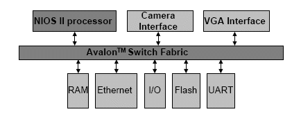
Figure. 2. Nios system
The Altera’s NIOS II softcore processor (FAST version) is a 32-bit scalar RISC processor with Harvard architecture, 6-stage pipeline, 1-way direct-mapped 64KB data cache, 1-way direct-mapped 64KB instruction cache and can execute up to 150 MIPS [2]. The main interest of this softcore processor is its extensibility and adaptability. Indeed, users can incorporate custom logic directly into the NIOS II Arithmetic Logic Unit (ALU). Furthermore, users can connect into the FPGA circuit the on-chip softcore processor and all custom peripherals to the bus. Thus, users can define their own instructions and processor peripherals to optimize the system for a specific application.
2.1. Camera interface
The general structure of the camera interface is presented by the following synoptic.
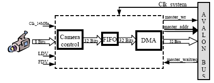
Figure. 3. Camera interface
This interface is based on three modules. The camera control module allows to send the acquired video data towards the FIFO (First In First Out) module with 32-Bits words. Indeed, in the purpose of using the 32-bit bus size, each four 8-bit data pixels must be processed at a 32-bit long word.
The FIFO allows to memorize an image line (640 pixels). It is like a buffer between the data writing and reading. Writing in the FIFO is synchronized with the camera clock. In the other hand, reading is synchronized with the system clock (120 MHz). Indeed, it is necessary that reading the FIFO data towards the SRAM is quite fast to follow the camera stream.
The third module is the DMA that allows the data transfer from the FIFO towards the SRAM through the Avalon bus by using «master_w», «master_addrw» and «master_wrdata» signals. The writing cycle extends until the Avalon bus activates «master_waitreq» signal.
2.2. VGA interface
The general structure of the VGA interface [3] is presented by the following figure.
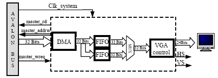
Figure. 4. Synoptic of the VGA interface
This interface uses three modules. The DMA module allows to transfer the data from the SRAM towards the FIFO by using «master_rd» (starting the reading of the master from the slave) and «master_addrw» (addresses sent towards the Avalon bus) signals.
A buffer module is composed of two FIFOs which have the same depth (640 pixels for one image line). Indeed, if the DMA writes in the first FIFO, the VGA controller module reads from the second FIFO. This last module sends « R », « G », « B » and synchronization signals to the VGA extension board (HS: Horizontal Synchronization signal and VS: Vertical Synchronization signal).
Writing in the FIFO is synchronized with the system clock (120 MHz). In the other hand, reading is synchronized with the VGA clock (25 MHz). The interface allows to transfer the 32-bit data from the Avalon bus towards the visualization VGA monitor.
2.3. Synchronization between the Camera and VGA interface
To allow image acquisition and image restitution,, the camera and the VGA interface must share the same SRAM slave. A problem may happen if the VGA and camera interfaces access SRAM at the same time. Synchronization is then necessary between these two interfaces which is presented by the flowchart below.
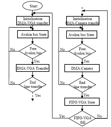
Figure. 5. Interfaces synchronization
As shown in Figure.5, an interface can begin a data transfer only if the other ends. In our case, the VGA interface has an higher priority since a data transfer discontinuity between the SRAM and the FIFO-VGA causes problems while displaying video. For this, the DMA-camera transfer starts only when the DMA-VGA transfer is finished.
3. HW/SW Codesign Exemple: H.263 Video Encoder
In order to optimize and achieve best performance for the H.263 video encoder in real-time [4], we have used the HW/SW codesign process. At first, the algorithms were coded in ANSI C programming language on a PC host. The tested SW code was then rebuilt and put into the Nios II system. The performance analysis with the CPU timer was used. Afterwards, the SW critical parts were implemented in HW with the VHDL language.
3.1. Overview of the H.263 Video Coding Standard
The block diagram of an H.263 baseline video encoder is shown in Figure.6. The encoder operation is based on a hybrid differential/transform coding, and is a combination of lossy and lossless coding. There are two fundamental modes which are jointly used for maximum compression efficiency: the intra and inter modes. The H.263 video encoder includes several blocks such as motion estimation (ME), Discrete Cosine Transform (DCT/IDCT), quantization (Q/IQ) and Variable Length Coding (VLC)
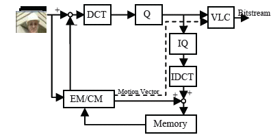
Figure. 6. Baseline H.263 video encoder
3.2. Timing analyses
In our experiments of coding a general video clip in QCIF format (Quarter Common Intermediate Format: Spatial resolution of 176x144 and temporal resolution 10 frames/s (fps)).
The average frame rate achieved on a NIOS II system is only 0.4 fps. For this reason, we investigated the resource distribution of the H.263 video coder which uses half-pixel full search motion estimation, search window size +/-15 and the quantization step QP=16. Figure.7 shows the distribution of the execution time for a testing sequence. In this figure, ME/MC and DCT/IDCT which use 61 % and 37 % of the execution time respectively are the two primary computationally intensive components. Thus, main purpose is to improve these two components using HW/SW codesign
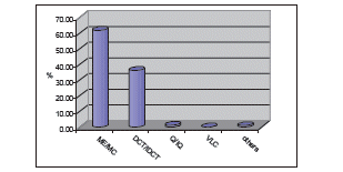
Figure. 7. Execution time distribution for QCIF sequence
The main idea of our coder is to exploit advantages of the parallel structures which can be efficiently implemented in hardware. Hardware implementation of 2-D DCT and 2-D IDCT (the Loeffler algorithm is used) [5] promises better results compared to software based algorithms. The key point of a parallel hardware structure is a reduced number of operations and the ability of parallel processing. However, there is still a good chance to reduce the complexity of the ME and MC in software by using fast motion estimation algorithms. The HEXBS [6] is the popular fast block-matching algorithm and it can reduce computational complexity.
3.3. FPGA implementation of the h.263 video encoder
The block diagram of the implemented H.263 encoder is shown in Figure.8. It is composed with five parts: the Nios II softcore processor, 2-D DCT and 2-D IDCT hardware cores and camera and VGA interfaces.
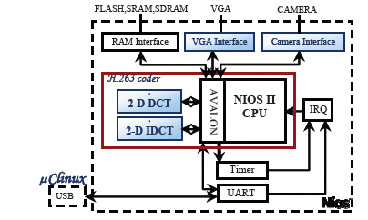
Figure. 8. Embedded video system
The whole project was executed under ìClinux with the Nios II softcore processor.
ìClinux is the main Embedded Linux Operating System port for processors without Memory Management Unit (MMUs). The ìClinux port for the Nios II core is licensed under the terms of the GNU General Public License (GPL) [7]. Our system receives frames from the camera and stores them into the external memory according to the camera rate. These frames are processed and compressed by the H.263 video encoder. Finally, the reconstructed frames are displayed on a monitor by the VGA controller.
3.4. 2-D DCT/IDCT coprocessor core
The 2-D DCT/IDCT transformation is implemented using the row/column approach which requires three steps: 8-point 1-D DCT/IDCT along the rows, memory transposition and another 8-point DCT/IDCT along the transposed columns. Figure. 9 is a block diagram of the 2-D DCT/IDCT coprocessor core, showing the main interface and functional blocks.
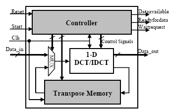
Figure. 9. 2-D DCT/IDCT coprocessor core
The controller is the control unit for the DCT/IDCT transformation. It receives input control signals (Reset, Start) and generates all the internal control signals for each stage and the output control signals for Avalon Bus communication (Dataavailable, Readyfordata, Waitrequest). When the Start signal is activated, the controller enables input of the first data row through Data_in signal. It then activates the 1-D DCT/IDCT unit for row data processing. The first row of the transpose memory stores the results in an intermediate memory. This process repeats for the remaining seven rows of the input block. Next, the 1-D DCT/IDCT unit receives input data from the columns of the transpose memory under the MUX. The results of the column-wise 1-D DCT/IDCT are available through the Data_out signal. Data_in and Data_out signals are connected to the Avalon Bus. The 2-D DCT/IDCT coprocessor read/store the data from/to SDRAM through this bus.
3.5. FPGA Implementation results
Table 1 shows implementation results of our video system in the Altera Stratix EP2S60 FPGA circuit which is based on a 90 nm technology, 1.2 V, with a density that reaches 48352 Adaptive Look-Up Tables (ALUTs), 310 KB of Embedded System Blocs (ESBs), 288 DSP blocks and 493 Input/Output Blocks (IOBs) [8]. Results in the Table 1 have been obtained with separate implementation of the particular modules (camera and VGA interface, 2-D DCT and 2-D IDCT coprocessor core).
Table1. The implementation results in Stratix II FPGA
The entire embedded system uses 20 % of the ALUTs, 46 % of the ESBs, 18 % of the DSP blocks and 37 % of the IOBs. We can see that there is enough free space for other applications. The whole design works at a 120 MHz system clock. The implementation of H.263 coder in the FPGA circuit gives us a System on Programmable Chip (SoPC).
4. Experiment Results
The prototyping board operates at 120 MHz, 8.33 ns delay for each coded data is required. The working frequency is limited by the FPGA device: the Stratix EP2S20F672C3 circuit. Our system receives images from the camera. Our simulations show up to 28 time speed improvement for the H.263 coding compared to the software based solution. The results before and after timing optimization are presented in Figure. 10. These results prove that after optimization, our H.263 coder can process 11 frames QCIF/sec which depend on the CPU clock frequency.
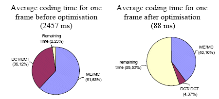
Figure. 10. CPU time percentage according to the processing before and after optimization
5. Conclusions
Based on a programmable technology (FPGA circuit, softcore processor), a powerful prototype platform for image processing was designed in order to support HW/SW codesign and partitioning. This platform allows flexible HW/SW implementation. A large spectrum of potential real-time imaging and video applications can be integrated.
6. References
[1] Nios II Development Kit, Stratix II
[2] Nios
[3] Lancelot Home Page, “VGA video controllerâ€
[4] ITU-T Rec. H.263, Video Coding for Low Bit Rate communication. 1998.
[5] Optimization and implementation on FPGA of the DCT/IDCT algorithm. A. Ben Atitallah, P. Kadionik, F. Ghozzi, P. Nouel, IEEE ICASSP '06, Toulouse, France, 14-19 mai 2006
[6] C. Zhu and al. , “Hexagon-Based Search Pattern for Fast Block Motion Estimationâ€, IEEE Trans. On Circuits And Systs, vol. 12, pp. 349-355, May 2002
[7] The NIOS Forum
[8] D.Lewis and Al, “The Stratix II Logic and Routing Architecture,†FPGA’05, February 20–22, 2005, Monterey, California, USA.
(1) Laboratory of Electronics and Information Technology, Tunisia
(2) IMS laboratory - ENSEIRB , France
Abstract:
This paper presents a dedicated hardware platform for a fast video and image data processing to real time application. The platform supports simultaneous HW/SW codesign and partitioning and based on the FPGA technologies and on a RISC processor. This reduces application design cycle. As an example, the H.263 video encoder is presented
1. Introduction
The necessity for real-time video processing capabilities in embedded systems is generally increasing with time. Real-time video processing is a very data intensive task when compared to many of the normal tasks performed by embedded systems. Even in simple real-time video operations where the algorithmic complexity of the processing is very low, the mere transfer of image data may consume significant system resources.
FPGAs provide an efficient alternative for implementing video processing applications. Modern FPGAs include many attractive characteristics such as: flexibility, low cost, high integration, embedded distributed memories and extensive parallelism. The main purpose of the paper is to practice of the HW/SW codesign process in FPGA. An efficient HW/SW codesign process is the key to design real-time embedded video system application.
This paper is organized as follow. Section 2 describes the embedded video system, the camera and VGA hardware interfaces. The implementation of the HW/SW codesign H.263 video encoder is presented then in section 3. The experiment results are presented in section 4. Section 5 concludes the paper.
2. Embedded Video System
In our video and image processing application, the chain contains acquisition module, processing and restitution of a video signal coming from the video source. The global processing video system is based on a System on Programmable Chip (SoPC): all system components are put into a single chip (FPGA). The synoptic diagram of the realized system is presented in Figure.1.

Figure. 1. Video System
For the main processing stage, the Altera NIOS II development board was chosen [1]. The core of the board is the Altera Stratix II EP2S60F672C3 FPGA circuit. Several peripheral devices and connectors serve as interfaces between the Stratix II FPGA circuit and the external environment. For our embedded system for video, we are using flash memory, SRAM, SDRAM, UART, timer, Ethernet, movie camera for image acquisition and VGA for image restitution. Our embedded system is composed with three IP modules: a NIOS II soft core processor, a camera interface and a VGA interface hardware core. The main processing core of our embedded system illustrated in figure 2, is the Nios II softcore processor. It is connected to hardware peripherals with the custom Altera’s Avalon bus.

Figure. 2. Nios system
The Altera’s NIOS II softcore processor (FAST version) is a 32-bit scalar RISC processor with Harvard architecture, 6-stage pipeline, 1-way direct-mapped 64KB data cache, 1-way direct-mapped 64KB instruction cache and can execute up to 150 MIPS [2]. The main interest of this softcore processor is its extensibility and adaptability. Indeed, users can incorporate custom logic directly into the NIOS II Arithmetic Logic Unit (ALU). Furthermore, users can connect into the FPGA circuit the on-chip softcore processor and all custom peripherals to the bus. Thus, users can define their own instructions and processor peripherals to optimize the system for a specific application.
2.1. Camera interface
The general structure of the camera interface is presented by the following synoptic.

Figure. 3. Camera interface
This interface is based on three modules. The camera control module allows to send the acquired video data towards the FIFO (First In First Out) module with 32-Bits words. Indeed, in the purpose of using the 32-bit bus size, each four 8-bit data pixels must be processed at a 32-bit long word.
The FIFO allows to memorize an image line (640 pixels). It is like a buffer between the data writing and reading. Writing in the FIFO is synchronized with the camera clock. In the other hand, reading is synchronized with the system clock (120 MHz). Indeed, it is necessary that reading the FIFO data towards the SRAM is quite fast to follow the camera stream.
The third module is the DMA that allows the data transfer from the FIFO towards the SRAM through the Avalon bus by using «master_w», «master_addrw» and «master_wrdata» signals. The writing cycle extends until the Avalon bus activates «master_waitreq» signal.
2.2. VGA interface
The general structure of the VGA interface [3] is presented by the following figure.

Figure. 4. Synoptic of the VGA interface
This interface uses three modules. The DMA module allows to transfer the data from the SRAM towards the FIFO by using «master_rd» (starting the reading of the master from the slave) and «master_addrw» (addresses sent towards the Avalon bus) signals.
A buffer module is composed of two FIFOs which have the same depth (640 pixels for one image line). Indeed, if the DMA writes in the first FIFO, the VGA controller module reads from the second FIFO. This last module sends « R », « G », « B » and synchronization signals to the VGA extension board (HS: Horizontal Synchronization signal and VS: Vertical Synchronization signal).
Writing in the FIFO is synchronized with the system clock (120 MHz). In the other hand, reading is synchronized with the VGA clock (25 MHz). The interface allows to transfer the 32-bit data from the Avalon bus towards the visualization VGA monitor.
2.3. Synchronization between the Camera and VGA interface
To allow image acquisition and image restitution,, the camera and the VGA interface must share the same SRAM slave. A problem may happen if the VGA and camera interfaces access SRAM at the same time. Synchronization is then necessary between these two interfaces which is presented by the flowchart below.

Figure. 5. Interfaces synchronization
As shown in Figure.5, an interface can begin a data transfer only if the other ends. In our case, the VGA interface has an higher priority since a data transfer discontinuity between the SRAM and the FIFO-VGA causes problems while displaying video. For this, the DMA-camera transfer starts only when the DMA-VGA transfer is finished.
3. HW/SW Codesign Exemple: H.263 Video Encoder
In order to optimize and achieve best performance for the H.263 video encoder in real-time [4], we have used the HW/SW codesign process. At first, the algorithms were coded in ANSI C programming language on a PC host. The tested SW code was then rebuilt and put into the Nios II system. The performance analysis with the CPU timer was used. Afterwards, the SW critical parts were implemented in HW with the VHDL language.
3.1. Overview of the H.263 Video Coding Standard
The block diagram of an H.263 baseline video encoder is shown in Figure.6. The encoder operation is based on a hybrid differential/transform coding, and is a combination of lossy and lossless coding. There are two fundamental modes which are jointly used for maximum compression efficiency: the intra and inter modes. The H.263 video encoder includes several blocks such as motion estimation (ME), Discrete Cosine Transform (DCT/IDCT), quantization (Q/IQ) and Variable Length Coding (VLC)

Figure. 6. Baseline H.263 video encoder
3.2. Timing analyses
In our experiments of coding a general video clip in QCIF format (Quarter Common Intermediate Format: Spatial resolution of 176x144 and temporal resolution 10 frames/s (fps)).
The average frame rate achieved on a NIOS II system is only 0.4 fps. For this reason, we investigated the resource distribution of the H.263 video coder which uses half-pixel full search motion estimation, search window size +/-15 and the quantization step QP=16. Figure.7 shows the distribution of the execution time for a testing sequence. In this figure, ME/MC and DCT/IDCT which use 61 % and 37 % of the execution time respectively are the two primary computationally intensive components. Thus, main purpose is to improve these two components using HW/SW codesign

Figure. 7. Execution time distribution for QCIF sequence
The main idea of our coder is to exploit advantages of the parallel structures which can be efficiently implemented in hardware. Hardware implementation of 2-D DCT and 2-D IDCT (the Loeffler algorithm is used) [5] promises better results compared to software based algorithms. The key point of a parallel hardware structure is a reduced number of operations and the ability of parallel processing. However, there is still a good chance to reduce the complexity of the ME and MC in software by using fast motion estimation algorithms. The HEXBS [6] is the popular fast block-matching algorithm and it can reduce computational complexity.
3.3. FPGA implementation of the h.263 video encoder
The block diagram of the implemented H.263 encoder is shown in Figure.8. It is composed with five parts: the Nios II softcore processor, 2-D DCT and 2-D IDCT hardware cores and camera and VGA interfaces.

Figure. 8. Embedded video system
The whole project was executed under ìClinux with the Nios II softcore processor.
ìClinux is the main Embedded Linux Operating System port for processors without Memory Management Unit (MMUs). The ìClinux port for the Nios II core is licensed under the terms of the GNU General Public License (GPL) [7]. Our system receives frames from the camera and stores them into the external memory according to the camera rate. These frames are processed and compressed by the H.263 video encoder. Finally, the reconstructed frames are displayed on a monitor by the VGA controller.
3.4. 2-D DCT/IDCT coprocessor core
The 2-D DCT/IDCT transformation is implemented using the row/column approach which requires three steps: 8-point 1-D DCT/IDCT along the rows, memory transposition and another 8-point DCT/IDCT along the transposed columns. Figure. 9 is a block diagram of the 2-D DCT/IDCT coprocessor core, showing the main interface and functional blocks.

Figure. 9. 2-D DCT/IDCT coprocessor core
The controller is the control unit for the DCT/IDCT transformation. It receives input control signals (Reset, Start) and generates all the internal control signals for each stage and the output control signals for Avalon Bus communication (Dataavailable, Readyfordata, Waitrequest). When the Start signal is activated, the controller enables input of the first data row through Data_in signal. It then activates the 1-D DCT/IDCT unit for row data processing. The first row of the transpose memory stores the results in an intermediate memory. This process repeats for the remaining seven rows of the input block. Next, the 1-D DCT/IDCT unit receives input data from the columns of the transpose memory under the MUX. The results of the column-wise 1-D DCT/IDCT are available through the Data_out signal. Data_in and Data_out signals are connected to the Avalon Bus. The 2-D DCT/IDCT coprocessor read/store the data from/to SDRAM through this bus.
3.5. FPGA Implementation results
Table 1 shows implementation results of our video system in the Altera Stratix EP2S60 FPGA circuit which is based on a 90 nm technology, 1.2 V, with a density that reaches 48352 Adaptive Look-Up Tables (ALUTs), 310 KB of Embedded System Blocs (ESBs), 288 DSP blocks and 493 Input/Output Blocks (IOBs) [8]. Results in the Table 1 have been obtained with separate implementation of the particular modules (camera and VGA interface, 2-D DCT and 2-D IDCT coprocessor core).
Table1. The implementation results in Stratix II FPGA
| Camera Interface | VGA Interface | 2-D DCT coprocessor | 2-D IDCT coprocessor | |
| ALUT | 1% | 1% | 3% | 3% |
| ESBs | 1% | 1% | 1% | 1% |
| DSPs | 0% | 0% | 8% | 8% |
| IOBs | 30% | 30% | 15% | 15% |
| Fmax (MHz) | 241 | 224 | 133 | 139 |
The entire embedded system uses 20 % of the ALUTs, 46 % of the ESBs, 18 % of the DSP blocks and 37 % of the IOBs. We can see that there is enough free space for other applications. The whole design works at a 120 MHz system clock. The implementation of H.263 coder in the FPGA circuit gives us a System on Programmable Chip (SoPC).
4. Experiment Results
The prototyping board operates at 120 MHz, 8.33 ns delay for each coded data is required. The working frequency is limited by the FPGA device: the Stratix EP2S20F672C3 circuit. Our system receives images from the camera. Our simulations show up to 28 time speed improvement for the H.263 coding compared to the software based solution. The results before and after timing optimization are presented in Figure. 10. These results prove that after optimization, our H.263 coder can process 11 frames QCIF/sec which depend on the CPU clock frequency.

Figure. 10. CPU time percentage according to the processing before and after optimization
5. Conclusions
Based on a programmable technology (FPGA circuit, softcore processor), a powerful prototype platform for image processing was designed in order to support HW/SW codesign and partitioning. This platform allows flexible HW/SW implementation. A large spectrum of potential real-time imaging and video applications can be integrated.
6. References
[1] Nios II Development Kit, Stratix II
[2] Nios
[3] Lancelot Home Page, “VGA video controllerâ€
[4] ITU-T Rec. H.263, Video Coding for Low Bit Rate communication. 1998.
[5] Optimization and implementation on FPGA of the DCT/IDCT algorithm. A. Ben Atitallah, P. Kadionik, F. Ghozzi, P. Nouel, IEEE ICASSP '06, Toulouse, France, 14-19 mai 2006
[6] C. Zhu and al. , “Hexagon-Based Search Pattern for Fast Block Motion Estimationâ€, IEEE Trans. On Circuits And Systs, vol. 12, pp. 349-355, May 2002
[7] The NIOS Forum
[8] D.Lewis and Al, “The Stratix II Logic and Routing Architecture,†FPGA’05, February 20–22, 2005, Monterey, California, USA.
