Wojciech Sakowski, Institute of Electronics, Silesian University of Technology
Abstract
This paper presents an instruction set simulator of a 32-bit CPU and explains its use in embedded software development. Interaction of the ISS with transaction level model of a complex peripheral (Firewireâ„¢ link layer controller) is also discussed.
Motivation
Electronic devices built nowadays are often built with a single integrated circuit composed of multitude of hardware blocks that implement the device functionality. In most cases such circuit contains one or more processors that enables to implement a part of the circuit functionality as a software that runs on that processor rather than as a specific hardware component.
Such IC is commonly referred to as a system-on-a-chip (SoC). Development of these complex chips is based on reuse and integration of formerly designed functional blocks (IP cores), available in the form of synthesizable RTL code written in VHDL or Verilog. Simulation of these synthesizable models is too slow to make use of them in software development. Therefore software developers have to wait until a hardware prototype is available or they need more abstract representation of SoC building blocks that could simulate circuit functionality – relevant to software development - much faster than RTL models. Instruction Set Simulators for processors and Transaction Level Models for other hardware blocks written in languages such as SystemC bring solution to these problems.
Processor core of which instruction set simulator is presented in this paper was developed originally as an obsolete part replacement. However its availability in the form of an IP core enabled development of systems-on-chip.
C68000_OCDS processor core
C68000_OCDS is an virtual component, designed at Evatronix company as an equivalent of MC68000â„¢ microprocessor once manufactured by Motorola and intended to be used in ASIC or FPGA implementations. The main CPU features are:
- 16-bit two-level instruction decoder cooperating with three-level deep instruction queue
- 55 instructions with 14 possible addressing modes
- Supervisor and user CPU with independent stack pointer registers
- Eight 32-bit data, eight 32-bit address and 16-bit status registers
- 16-bit external memory interface selectable 23/32-bit address bus; there is also version of this core available that is equipped with full 32-bit AMBA interface
- Seven priority level interrupt controller with vectored and auto-vectored modes
To facilitate embedded software development process, the On-Chip Debug System (OCDS) was incorporated into C68000_OCDS, providing set of features that allow to control program flow and CPU state introspection:
- Run / stop / step control
- Register read / write access
- Memory read / write ability
- Configurable and flexible data access breakpoints
- Unlimited number of software code breakpoints
C68K_ISS – overview and model features
C68K_ISS is a transaction-level model of C68000_OCDS IP-core. It was developed to be the Instruction-Set Simulator of the original CPU.
Main assumptions for the ISS were:
- Developed in pure C++ language for high performance and portability (e.g. to use ISS as plug-in for the third-party debuggers)
- External SystemC wrapper with interfaces to connect external components
- Single-instruction accuracy, without taking internal architecture under consideration
- Fully static design with neither internal processes nor loop / wait statements
- Usage of native C++ types to gain high simulation speed
- Optimized instruction decoder using lookup tables for high performance and easy extensibility
- Pure PV model without internal time dependencies
- Communication interfaces separated from functionality
Architecture description
Model consists of six internal sub-components, as figure 1 shows.
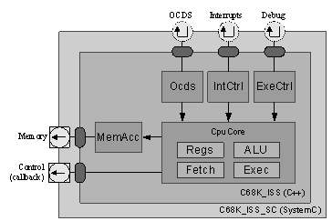
Fig. 1 Architecture of C68000_ISS
The main part is the CpuCore, which contains implementation of main processor’s logic (ALU, instruction fetch, decoding and execution routines) together with fields corresponding to the internal resources (all registers). Sub-module features:
- Fetching and decoding instructions
- Instruction processing routines
- Handling interrupts and exceptions
- Register implementation and registers read/write access
- Instruction counter
The second sub-module is the MemAcc one; it is responsible to provide communication with the external memory. All data breakpoint logic is implemented in this module. Features:
- Centralized external memory access
- Data breakpoint
ExeCtrl module implements debug functionality – like run, step, stop, register memory access and other flow control / CPU state introspection routines. It also provides external interface to inform the environment about particular events (like CPU start / stop or external devices reset). Features summary:
- CPU reset and initialization
- Start / stop routines (with multi-thread support)
- Single / several instructions step
- Internal CPU registers read / write
- CPU external memory read / write
- Data breakpoint configuration
- CPU callbacks to the environment
Interrupts are received and initially handled by the IntCtrl sub-module – it resolves priority of incoming request and – if accepted – passes it to the main module. Features:
- Vectored / auto-vectored interrupt requests reception
- Priority resolving (IPL comparison)
OCDS unit implements functionality provided in C68000_OCDS by the On-Chip Debug System run/step/stop routines, breakpoints and register/memory access. Since all the functionality needed by the OCDS is distributed among other modules, it acts as central point for controlling the CPU. OCDS features (subset of debug ones implemented in ExeCtrl module) are listed below:
- CPU reset and initialization
- Instruction flow control (run / stop / step)
- Read / write CPU registers
- Read / write memory (through CPU)
- Data breakpoint handling
- Instruction insertion and execution
All sub-modules are written in pure C++ and communication between them is done by the means of interface pointers (each component has its own interface class that contains published routines). Modules are gathered by the top-level class (named CC68kIss), which exports appropriate functionality through pointers. Interface classes are listed below (master and slave are assigned from ISS point of view):
- ICppDebug – debug interface (slave)
- ICppMemAcc – external memory access (master)
- ICppIntReq – interrupt request (slave)
- ICppCallback – internal CPU events callback (master)
- IC68kGenOcds – OCDS features (slave)
SystemC interfaces simply derive from generic C++ interface class and from sc_interface, as listed below:
- IScDebug inherits directly from C++ interface ICppDebug
- IPvBusData from ICppMemAcc
- ITlmIntReq from ICppIntReq
- IScCallback from ICppCallback
- IC68kOcds from IC68kGenOcds
SystemC top-level (CC68kIssSc) is implemented in the same way, except that inherits not only from sc_module and C++ ISS class, but also from all slave interface classes (needed to implement appropriate sc_exports).
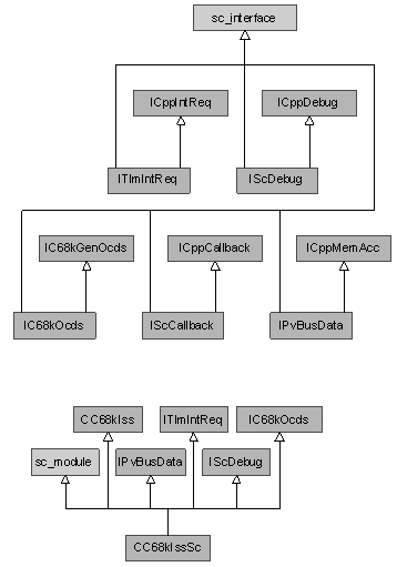
Fig. 2 Hierarchy of classes used in ISS development
Architecture details
Instruction decoder
The main performance limit in ISS models is instruction decoder. In many cases hard-coded if switch solution is used, which has the main drawback – in most cases op-code must be passed through several if branches, which is quite time consuming. Also debugging and extending (e.g. when implementing new instructions) is difficult. C68K_ISS uses look-up table approach – each instruction is fully identified by its first word, the following ones (if exist) can denote only instruction data or extended addressing parameters. In order to make fast decoder an instruction descriptor structure is prepared – it holds:
- Instruction kind
- Total instruction length (in words)
- Member pointer to the method responsible for instruction processing
- Optional source and destination addressing modes together with register indexes
- Additional instruction parameters
Such descriptors form one array with length of 65536, which is indexed by the first instruction word, and thus all necessary parameters (even addressing modes together with involved register index) are known immediately after first word is fetched from the code memory; the array is filled in automatic way (using bit masking) and – as a static ISS class field – it is shared among all C68K_ISS instances. Figure 3 shows a scheme of instruction decoding.
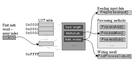
Fig. 3 Instruction decoding scheme
External memory access
External memory is accessed in two ways, depending on selected model (pure C++ / SystemC):
- For pure C++ model, memory is accessible through functional interface of ICppMemAcc, which contains routines like:
- ReadMem(addr, out_data, width, space)
- WriteMem(addr, data, width, space)
and their more advanced versions intended to perform block transfers, Pointer to this interface is stored in MemAcc module.
- SystemC model communicates with the memory through communication channel that uses tlm_transport_if with appropriately developed request and response structures (for low-level transmission) together with user-level functional interface.
Since SystemC model is made as child class of C68kIss, it was necessary to connect C++ memory access port to the SystemC one – appropriate routines are implemented in SystemC wrapper, as figure 4 shows.
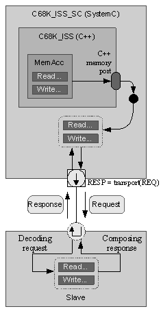
Fig. 4 Interaction of ISS with external memory
Data breakpoints
Data breakpoint logic is implemented in MemAcc sub-module. Breakpoint itself is described by the descriptor, which contains all data necessary to check whether memory access should trigger it:
- Address range
- Data value (together with mask)
- Address space (together with mask)
- Access type (read / write)
Descriptors are gathered into the array, which size can be dynamically changed at run-time. When memory access is performed, all descriptors are iterated in the loop to check if trigger conditions are met and – if so – CPU is stopped and callback (through callback port) is passed to the environment.
Testing environment
In order to verify C68K_ISS functional correctness appropriate testing environment was built, where SystemC model was run in co-simulation together with C68000_OCDS component. Both CPUs are running the same program, and after each instruction internal state (register values) and memory accesses were compared. C68000_OCDS was communicated using appropriate transactors (one for C68OOO ports and one for JTAG ports to communicate incorporated OCDS module).
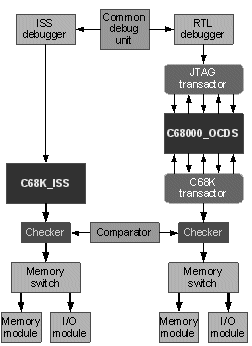
Fig. 5 Debugging environment for ISS making use of existing RTL description of the CPU
Performance analysis
After ISS module was fully verified, the performance tests were performed.
Execution environment
Tests were performed on AMD Sempron 2800+ with 1 GB RAM, running Windows XP operating system. Model was compiled using GCC 3.2.3.
Test results
After tests were completed, the following results were achieved:
- Pure C++ model – aprox. 2.5 M instructions per second
- SystemC model – aprox. 1.25 M instructions per second
The difference comes from the way of interfacing external memory, which is bottleneck for SystemC module – packing access into request structure and returning response object (together with necessary constructors / destructors call) are far more expensive than simple function call through interface pointer.
Interfacing ISS with the TLM model
C68K_ISS was intended to ease embedded software developing and verification process. To speed up simulation process, ISS should be connected with a TLM PV model.
Adaptation
C1394A_TLM model needed some simple preparations to connect to the ISS module:
- Bus wrapper was developed to the TLM functional SFR interface of 1394A_TLM.
- Then interrupt handling interface was modified to fit to the interrupt controller.
- Appropriate BFM was connected to the PHY interface of C1394A_TLM.
Software stack
Some parameters of C1394A Software Stack (regarding C1394A mapping address) needed to be configured. Then simple I / O printf routines were added to the application code for demonstration purpose. After all necessary changes were made, the stack was compiled for MC68000 architecture -linker produced Motorola S-Record file, which was input to the parser connected to the memory modules in environment.
Environment
Environment consists of:
- C68K_ISS module
- Memory switch
- Memory module
- Text I/O component
- VGA output module
- C1394A_TLM model
- 1394-bus BFM
- S-Record files parser
- Simulation control unit
Figure 6 shows environment components interconnections.
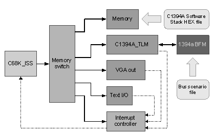
Fig. 6 Interaction of ISS with TLM of Firewireâ„¢ link layer controller
Application
For the testing purposes, user application was prepared – it grabs information (the Configuration ROM contents) from all the nodes connected to the bus and prints acquired information to the I/O (implemented as memory-mapped text file output). Information is updated and re-sent after each Bus Reset. Some random asynchronous and isochronous transmissions are also performed.
Simulation
During simulation system behaves as expected – bus topology was read from incoming Self-ID packets, the information was processed internally by the Software Stack and then put (by means of printf function) to the I/O module, which stores byte stream into text file and (optionally) to the simulation console.
Problems
The source of the problems was both integration (there was need to adapt C1394A_TLM SFR and interrupt interface to the ISS one) and application debugging, since no external debugger was attached to the system. As far as integration is concerned, the main problem were internal communication and sc_events, which introduce one-delta delay, so ISS control thread must have been enriched by the appropriate synchronization points. Next, lack of external debugger was not very burdensome, as the Software Stack was well verified, and simple integration tests were performed just to validate C68K_ISS – C1394A_TLM interconnections.
Conclusions
Developed ISS model allows extending embedded software verification process by details coming from exact target architecture (in opposition to native compilation mode) with a little performance degradation (compared to RTL simulation). Also simulation speed can be improved by exchanging C68000_OCDS to the ISS in SoCs in cases, where CPU architectural details exploration are not main simulation goal. Gained performance results (an over 10 times higher speed of ISS model in pure C++ environment in compare to SystemC one) shown, than it is very important to optimize external data communication channel.
Literature
1. M68000 Programmer’s Reference Manual, Motorola, 1992
2. C68000 Synthesizable HDL Core Specification, © Evatronix SA, 2002
3. C68000-OCDS On-Chip Debug Support, Specification, © Evatronix SA, 2004
4. IEEE Std 1394-1995
5. IEEE Std 1394a-2000
6. C1394A Design Specification, © Evatronix SA, 2004
7. Transaction Level Model Of IEEE 1394 Serial Bus Link Layer Controller Ip Core And Its Use In The Software Driver Development, Filip Rak, Wojciech Sakowski, Proceedings of IP-SoC 2005 Conference
8. SystemC: From the Ground Up, David C. Black, Jack Donovan, Kluwer Academic Publishers, 2004
