Srinivasan Nachiappan and Santosh Shivadatta
MindTree Consulting Ltd
Abstract
This paper describes the development of a configurable SoC platform using configurable IP cores, which is designed for low cost, low power and targeted for Bluetooth® and ULP (Ultra Low Power) Bluetooth standalone applications. The paper details the configurable SoC IP infrastructure, efficient co-verification methodology, and validation platform and automation framework.
Introduction to Bluetooth® Technology
Bluetooth® is a short range wireless communication technology intended to replace cables for portable/fixed devices. Bluetooth® technology operates in unlicensed 2.4 GHz ISM band and employs frequency hopping technique. Typical applications of Bluetooth® technology include hand sets, head sets, hands free units, HID’s (mouse, keyboards, remotes), note books, printers etc. Based on the IMS research report from 2006, the Bluetooth® market is expected to grow over 1.7 billion units by 2011 and the market share of the various applications is shown in the pie chart below.

Apart from the hand set market, the head set, hands free and the HID’s together have the next major market share of the technology. The ULP Bluetooth® technology intends to extend Bluetooth® wireless technology to end devices like watches, medical wellness equipments, sports and fitness equipments etc. These market segments together, demand a low cost, low power approach for implementing standalone Bluetooth® functionality in the end products. The product manufactures and component providers may deploy any of the following approaches for implementing Bluetooth® functionality in such Bluetooth centric end products.
Adding a Bluetooth® Module
This is the easiest and fastest time-to market solution but is an expensive and inflexible approach.
System-In-Package using Pre-Qualified Chip Sets
This is the most popular method adopted by system architects due to its inherent advantages of faster time-to-market with guaranteed performance and interoperability. But this method also offers very little engineering flexibility to achieve a low cost solution.
Develop Custom SoC’s using Configurable SoC Platform
A configurable Bluetooth® SoC platform is a bouquet of SoC IP infrastructure, verification environment, validation platform, and automation framework. This platform provides maximum engineering flexibility to achieve optimized area, power and memory foot print for a Bluetooth application thus providing a low cost solution.
Attributes of Bluetooth® Systems
Typical applications of Bluetooth® technology include portable devices while ULP Bluetooth® technology includes wearable devices. Such applications require interoperable, easy to use and affordable components. Longer battery life and longer range are also becoming critical with these portable/wearable end products. Bluetooth® systems designed for such applications demand a low cost, low power and highly flexible solution. Most of the standalone applications require a simple low performance processor subsystem.
Configurable SoC Platform
The configurable SoC platform comprises of configurable IP infrastructure, co-verification environment, validation platform and automation framework as detailed in the following sections.
SoC IP Infrastructure
The SoC IP infrastructure provides a configurable IP suite for building the custom SoC. The key aspects of this IP infrastructure are described below.
Bus Architecture
The platform supports AMBA bus architectures, the most popular on-chip bus communication standard. The AMBA AHB is supported for high-performance system modules like Bluetooth IP, which are required to run the core software engine. The AMBA APB is for low performance, peripheral modules used mostly by the applications.
The platform can be configured to support one AHB master and up to four AHB slaves. The AHB master in the platform is any industry standard processor core which supports AHB master interface. An AHB bus controller handles wait states inserted for the slow running AHB and APB peripherals. The following peripherals are connected to AHB bus considering the high performance requirements.
Memory Architecture
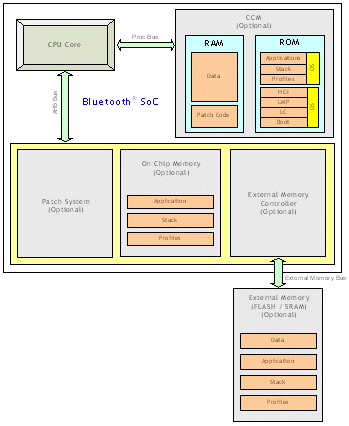
The platform supports the following optional AHB peripherals which are used to build various memory subsystems based on the application requirements.
Closely Coupled Memory Subsystem
In this configuration, the code memory (ROM) and the data memory (RAM) are closely integrated with the processor core. Closely coupled memories (Caches/TCM’s/CCM’s) provide the maximum performance as there is zero latency in code and data memory accesses. In this configuration none of the above memory subsystem related peripherals are required in the platform.
On-Chip Memory Subsystem
In this configuration, the code and data memories are accessed as AHB peripherals. The on chip memory controller provides a zero wait state access to these memories.
On-Chip/External Memory Subsystem
In this configuration, the code resides both in the on-chip and external memory. The time critical code can reside in the on-chip memory and the not so time critical code (application & profiles) can reside in the external memory. This gives the flexibility for the system architect to customize the platform for various applications.
Patch Subsystem
This configuration complements the Closely Coupled/On-Chip/External Memory subsystems by providing a method to de-risk the code (ROM) freeze.
Power Management
The platform supports a centralized system controller which provides the power management framework for the SoC. The peripheral IP’s also provides individual power management framework at an IP level. The software can exercise the power management framework to achieve optimal power consumption.
The system controller employs the following power management techniques.
IP Portfolio
The platform supports the following list of configurable IP’s which provides the flexibility to customize the IP’s based on the application requirements. The salient features of the IP’s are detailed below.
Bluetooth Base Band Controller
The base band controller IP comprising of both hardware and software components provides the Bluetooth® functionality. The hardware IP component provides a comprehensive feature set which can be configured based on the application. It also provides a configurable bus interface to ease SoC integration, radio and codec interface to support multiple vendors. The base band software component provides flexibility in porting across platforms, operating systems and provides a configurable transport layer.
GPIO
The GPIO IP provides the MMI (Man Machine Interface) for the system and can be configured up to 24 ports. The IP provides flexible pin multiplexing options for various special functions which results in optimal number of I/O’s for the SoC. It provides configurable options for I/O logic level, long & short press, pull up & pull down controls and de-bouncing circuitry.
Timer/Watch Dog Timer
The timer/watch dog timer IP provides the base timers used by the software and watch dog functionality. The IP can be configured for timer/ watch dog timer functionality, reset/interrupt generation and one-shot/cyclic mode of operation.
System Controller
The system controller IP provides the reset control and power management framework for the SoC. It employs dynamic clock gating, clock switching, frequency scaling and oscillator control features which the software can exercise to achieve optimal power consumption.
Interrupt Controller
The interrupt controller IP controls the interrupt scheme in the SoC. Up to 32 interrupts can be configured with individual programmable input/output interrupt mode/logic levels. It also provides the flexibility to be configured for normal/fast mode or individual interrupt mode based on the processor core.
On-Chip Memory Controller
The on chip memory controller IP provides the ROM/RAM interface for the on-chip memories. It supports 8/16 or 32 bit width accesses and zero wait states for memory accesses.
External Memory Controller
The external memory controller IP supports up to two external memory devices with cumulative memory space up to 4 MB. The IP can be configured to support 8/16 or 32 bit accesses with memory configurations of 8/16 or 32 bit data widths. It provides configurable memory access time parameters and logic levels for memory interface controls.
Patch System
The patch system IP complements memory subsystem by providing a method to de-risk the code (ROM) freeze and supports up to 16 patches.
UART
The UART IP provides the HCI transport layer functionality for Bluetooth® dongle applications and facilitates BQB qualification. The IP provides programmable baud rate generation up to 1Mbps, independent TX/RX buffers with programmable threshold settings, configurable flow control and interrupt modes.
SPI
The serial peripheral interface IP is used to interface with external SPI EEPROM which may encapsulate the Bluetooth® device related parameters, radio configurations etc. It can also contain the patch code which can be copied to the on-chip RAM and executed. The IP can be configured for 3/4 wire interface, different address/data widths/formats and interrupt modes.
I2C
The I2C IP is used to interface with external I2C EEPROM which may encapsulate the Bluetooth® device related parameters, radio configurations etc. It can also contain the patch code which can be copied to the on-chip RAM and executed. The IP can be configured for master/slave mode and different interrupt modes.
SoC Verification/Validation Infrastructure
The SoC verification/validation infrastructure provides the framework to verify and validate the customized SoC. The key aspects of the verification/validation infrastructure are described below.
Hardware Software Co-Verification
The hardware software co-verification is a C-based environment used for the verification of the application drivers and the peripheral IP’s & SoC aided by VPI (Verification Platform Interface) and TRM (Test Re-Use) methodologies. The VPI methodology provides the necessary verification stubs in the environment for effective test bench control and logging. The TRM methodology encourages the use of common drivers for test cases & application development and common test cases for verification & validation of peripherals. The environment also provides the following integrated model suite for various system configuration scenarios.
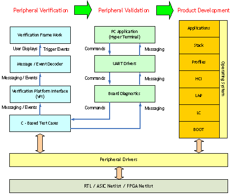
Validation Platform
The validation platform is a compact application development & prototyping platform which allows users to develop, validate and qualify (ULP) Bluetooth® solutions for diverse applications. The platform allows users to integrate & validate new peripherals and associated drivers, develop SoC & application software and perform the system level validation before targeting for an ASIC. The platform based on Xilinx Virtex II Pro FPGA family can be both battery (rechargeable) and adaptor operated. The platform supports on-board radio and expansion connectors for daughter cards to validate (ULP) Bluetooth® solutions for diverse applications. The platform also provides comprehensive debug and test support.
Automation Framework
The automation framework integrates the design, verification and validation infrastructure providing a user friendly environment for system development team. The automation framework enables variant SoC architecture evaluation at ease, integrates various stages in the system design flow thus significantly improving the productivity The key attributes of the automation framework are listed below.
AlphaBlue SoC platform is the configurable SoC platform developed based on the methodology described earlier. The platform is used to develop optimized SoC’s for Bluetooth® and ULP Bluetooth and device applications. The architecture of AlphaBlue SoC platform is shown below.
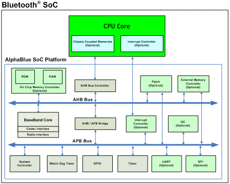
The co-verification environment for AlphaBlue SoC platform is shown below.
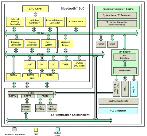
The FPGA validation platform developed for validating AlphaBlue SoC platform is shown below. The following Bluetooth® systems are validated using this platform.

Conclusion
Configurable SoC platform based approach provides maximum flexibility for the system architects to provide low cost solutions for (ULP) Bluetooth® end device applications. The approach also significantly reduces re-engineering effort incurred during variant SoC development for diverse applications. The approach enables faster prototyping of (ULP) Bluetooth® systems and time-to-market.
MindTree Consulting Ltd
Abstract
This paper describes the development of a configurable SoC platform using configurable IP cores, which is designed for low cost, low power and targeted for Bluetooth® and ULP (Ultra Low Power) Bluetooth standalone applications. The paper details the configurable SoC IP infrastructure, efficient co-verification methodology, and validation platform and automation framework.
Introduction to Bluetooth® Technology
Bluetooth® is a short range wireless communication technology intended to replace cables for portable/fixed devices. Bluetooth® technology operates in unlicensed 2.4 GHz ISM band and employs frequency hopping technique. Typical applications of Bluetooth® technology include hand sets, head sets, hands free units, HID’s (mouse, keyboards, remotes), note books, printers etc. Based on the IMS research report from 2006, the Bluetooth® market is expected to grow over 1.7 billion units by 2011 and the market share of the various applications is shown in the pie chart below.

Apart from the hand set market, the head set, hands free and the HID’s together have the next major market share of the technology. The ULP Bluetooth® technology intends to extend Bluetooth® wireless technology to end devices like watches, medical wellness equipments, sports and fitness equipments etc. These market segments together, demand a low cost, low power approach for implementing standalone Bluetooth® functionality in the end products. The product manufactures and component providers may deploy any of the following approaches for implementing Bluetooth® functionality in such Bluetooth centric end products.
Adding a Bluetooth® Module
This is the easiest and fastest time-to market solution but is an expensive and inflexible approach.
System-In-Package using Pre-Qualified Chip Sets
This is the most popular method adopted by system architects due to its inherent advantages of faster time-to-market with guaranteed performance and interoperability. But this method also offers very little engineering flexibility to achieve a low cost solution.
Develop Custom SoC’s using Configurable SoC Platform
A configurable Bluetooth® SoC platform is a bouquet of SoC IP infrastructure, verification environment, validation platform, and automation framework. This platform provides maximum engineering flexibility to achieve optimized area, power and memory foot print for a Bluetooth application thus providing a low cost solution.
Attributes of Bluetooth® Systems
Typical applications of Bluetooth® technology include portable devices while ULP Bluetooth® technology includes wearable devices. Such applications require interoperable, easy to use and affordable components. Longer battery life and longer range are also becoming critical with these portable/wearable end products. Bluetooth® systems designed for such applications demand a low cost, low power and highly flexible solution. Most of the standalone applications require a simple low performance processor subsystem.
Configurable SoC Platform
The configurable SoC platform comprises of configurable IP infrastructure, co-verification environment, validation platform and automation framework as detailed in the following sections.
SoC IP Infrastructure
The SoC IP infrastructure provides a configurable IP suite for building the custom SoC. The key aspects of this IP infrastructure are described below.
Bus Architecture
The platform supports AMBA bus architectures, the most popular on-chip bus communication standard. The AMBA AHB is supported for high-performance system modules like Bluetooth IP, which are required to run the core software engine. The AMBA APB is for low performance, peripheral modules used mostly by the applications.
The platform can be configured to support one AHB master and up to four AHB slaves. The AHB master in the platform is any industry standard processor core which supports AHB master interface. An AHB bus controller handles wait states inserted for the slow running AHB and APB peripherals. The following peripherals are connected to AHB bus considering the high performance requirements.
- Base Band Controller
- AHB to APB Bridge
- On-Chip Memory Controller
- External Memory Controller
- System Controller
- Timer
- Watch Dog Timer
- GPIO
- UART
- SPI
- I2C
- Interrupt Controller
- External Memory Controller
- Patch System
| Processor Core | AHB Bus | APB Bus |
| Freq | Freq | Freq |
| Freq | Freq | Freq/2 |
| Freq | Freq/2 | Freq/2 |
| Freq | Freq/2 | Freq/4 |
Memory Architecture
The platform supports the following optional AHB peripherals which are used to build various memory subsystems based on the application requirements.
- On-Chip Memory Controller
- External Memory Controller
- Patch System
Closely Coupled Memory Subsystem
In this configuration, the code memory (ROM) and the data memory (RAM) are closely integrated with the processor core. Closely coupled memories (Caches/TCM’s/CCM’s) provide the maximum performance as there is zero latency in code and data memory accesses. In this configuration none of the above memory subsystem related peripherals are required in the platform.
On-Chip Memory Subsystem
In this configuration, the code and data memories are accessed as AHB peripherals. The on chip memory controller provides a zero wait state access to these memories.
On-Chip/External Memory Subsystem
In this configuration, the code resides both in the on-chip and external memory. The time critical code can reside in the on-chip memory and the not so time critical code (application & profiles) can reside in the external memory. This gives the flexibility for the system architect to customize the platform for various applications.
Patch Subsystem
This configuration complements the Closely Coupled/On-Chip/External Memory subsystems by providing a method to de-risk the code (ROM) freeze.
Power Management
The platform supports a centralized system controller which provides the power management framework for the SoC. The peripheral IP’s also provides individual power management framework at an IP level. The software can exercise the power management framework to achieve optimal power consumption.
The system controller employs the following power management techniques.
- Dynamic Clock Gating
- Processor/Bus/Peripheral
- Dynamic Clock Switching
- System Clock/Low Power Clock
- Radio Clock/Low Power Clock
- Dynamic Frequency Scaling
- Processor/AHB/APB Clock Ratios
- External Oscillator / Crystal Controls
- System Clock/Low Power Clock
- Radio Clock/Codec Clock
- VDD Controls

IP Portfolio
The platform supports the following list of configurable IP’s which provides the flexibility to customize the IP’s based on the application requirements. The salient features of the IP’s are detailed below.
Bluetooth Base Band Controller
The base band controller IP comprising of both hardware and software components provides the Bluetooth® functionality. The hardware IP component provides a comprehensive feature set which can be configured based on the application. It also provides a configurable bus interface to ease SoC integration, radio and codec interface to support multiple vendors. The base band software component provides flexibility in porting across platforms, operating systems and provides a configurable transport layer.
GPIO
The GPIO IP provides the MMI (Man Machine Interface) for the system and can be configured up to 24 ports. The IP provides flexible pin multiplexing options for various special functions which results in optimal number of I/O’s for the SoC. It provides configurable options for I/O logic level, long & short press, pull up & pull down controls and de-bouncing circuitry.
Timer/Watch Dog Timer
The timer/watch dog timer IP provides the base timers used by the software and watch dog functionality. The IP can be configured for timer/ watch dog timer functionality, reset/interrupt generation and one-shot/cyclic mode of operation.
System Controller
The system controller IP provides the reset control and power management framework for the SoC. It employs dynamic clock gating, clock switching, frequency scaling and oscillator control features which the software can exercise to achieve optimal power consumption.
Interrupt Controller
The interrupt controller IP controls the interrupt scheme in the SoC. Up to 32 interrupts can be configured with individual programmable input/output interrupt mode/logic levels. It also provides the flexibility to be configured for normal/fast mode or individual interrupt mode based on the processor core.
On-Chip Memory Controller
The on chip memory controller IP provides the ROM/RAM interface for the on-chip memories. It supports 8/16 or 32 bit width accesses and zero wait states for memory accesses.
External Memory Controller
The external memory controller IP supports up to two external memory devices with cumulative memory space up to 4 MB. The IP can be configured to support 8/16 or 32 bit accesses with memory configurations of 8/16 or 32 bit data widths. It provides configurable memory access time parameters and logic levels for memory interface controls.
Patch System
The patch system IP complements memory subsystem by providing a method to de-risk the code (ROM) freeze and supports up to 16 patches.
UART
The UART IP provides the HCI transport layer functionality for Bluetooth® dongle applications and facilitates BQB qualification. The IP provides programmable baud rate generation up to 1Mbps, independent TX/RX buffers with programmable threshold settings, configurable flow control and interrupt modes.
SPI
The serial peripheral interface IP is used to interface with external SPI EEPROM which may encapsulate the Bluetooth® device related parameters, radio configurations etc. It can also contain the patch code which can be copied to the on-chip RAM and executed. The IP can be configured for 3/4 wire interface, different address/data widths/formats and interrupt modes.
I2C
The I2C IP is used to interface with external I2C EEPROM which may encapsulate the Bluetooth® device related parameters, radio configurations etc. It can also contain the patch code which can be copied to the on-chip RAM and executed. The IP can be configured for master/slave mode and different interrupt modes.
SoC Verification/Validation Infrastructure
The SoC verification/validation infrastructure provides the framework to verify and validate the customized SoC. The key aspects of the verification/validation infrastructure are described below.
Hardware Software Co-Verification
The hardware software co-verification is a C-based environment used for the verification of the application drivers and the peripheral IP’s & SoC aided by VPI (Verification Platform Interface) and TRM (Test Re-Use) methodologies. The VPI methodology provides the necessary verification stubs in the environment for effective test bench control and logging. The TRM methodology encourages the use of common drivers for test cases & application development and common test cases for verification & validation of peripherals. The environment also provides the following integrated model suite for various system configuration scenarios.
- SPI/I2C EEPROM
- SRAM/FLASH
- Codec
- Bluetooth® Radio/Air
- Protocol Checkers/Monitors

Validation Platform
The validation platform is a compact application development & prototyping platform which allows users to develop, validate and qualify (ULP) Bluetooth® solutions for diverse applications. The platform allows users to integrate & validate new peripherals and associated drivers, develop SoC & application software and perform the system level validation before targeting for an ASIC. The platform based on Xilinx Virtex II Pro FPGA family can be both battery (rechargeable) and adaptor operated. The platform supports on-board radio and expansion connectors for daughter cards to validate (ULP) Bluetooth® solutions for diverse applications. The platform also provides comprehensive debug and test support.
Automation Framework
The automation framework integrates the design, verification and validation infrastructure providing a user friendly environment for system development team. The automation framework enables variant SoC architecture evaluation at ease, integrates various stages in the system design flow thus significantly improving the productivity The key attributes of the automation framework are listed below.
- Compiler and Simulator Integration
- Memory Subsystem Configurations
- Peripheral Configurations
- ASIC/FPGA Configurations
- RTL/Gate Level Simulations
- Regression/Standalone/Debug Control
- FPGA Synthesis & PNR Configurations
- ASIC Synthesis & Static Timing Analysis
AlphaBlue SoC platform is the configurable SoC platform developed based on the methodology described earlier. The platform is used to develop optimized SoC’s for Bluetooth® and ULP Bluetooth and device applications. The architecture of AlphaBlue SoC platform is shown below.

The co-verification environment for AlphaBlue SoC platform is shown below.

The FPGA validation platform developed for validating AlphaBlue SoC platform is shown below. The following Bluetooth® systems are validated using this platform.
- Hands Free
- Remote Control

Conclusion
Configurable SoC platform based approach provides maximum flexibility for the system architects to provide low cost solutions for (ULP) Bluetooth® end device applications. The approach also significantly reduces re-engineering effort incurred during variant SoC development for diverse applications. The approach enables faster prototyping of (ULP) Bluetooth® systems and time-to-market.
