By Hany G. Bakeer, Omar Shaheen, Haitham M. Eissa from Mentor Graphics
Abstract:
A well planned verification flow for a mixed-signal IP is required to achieve the highest quality of the IP performance with the expected design specifications. The aim of this paper is to present a mixed-signal verification flow for the Universal Serial Bus physical layer IP. The verification flow for both the analog and digital blocks in the USB2.0 PHY are presented. A combined mixed-signal system level verification flow for the whole IP is introduced. Examples for different test benches required to verify the USB2.0 PHY IP is presented with some illustration results.
1. Introduction
The increasing complexity of the end product electronics systems; put more challenges on the engineering design groups to meet shorter time-to-market with the highest required quality. Using Intellectual Property designs is one of the solutions that could help end-product designers to quickly integrate and assemble their complex systems using different IPs. However the main concern for system engineers is the quality of the IP and how good it will perform as expected within their systems. This makes IP verification one of the most challenging issues for IP designers. Considering the fact that the IP could be integrated into any unknown system or environment; this makes the scope of the IP verification plan wider and to consider any possible different scenarios for IP/System integration. One of the common used IPs in the market is the Universal Serial Bus IP. Since its release in 1995; the USB interface proves to be one of the most successful interfaces for serial data transfers. The first USB 1.x data transfer rates were at Low-Speed 1.5Mbps & Full-Speed 12Mbps. These data rates were good enough for low and medium speed applications such as computer peripherals and flash memory storage drives. The success of USB 1.x and the growing market demand for high speed data applications; paved the way for USB 2.0; released by the USB-IF in 2001 [1]. The High-Speed USB 2.0 data transfer rate is 480 Mbps. USB 2.0 is now a common port in almost all multimedia and portable applications such as portable MP3 players, digital cameras, video camcorders, gaming consoles and even TV sets now have a USB port. The growing expansion of the multimedia market will require higher data rate transfers for larger multimedia files. The Super-Speed USB 3.0 initial proposal are already out there with 10x faster than USB 2.0 and a data rate of 4.8Gbps [2].
Considering the USB physical layer; the USB PHY consists of both analog and digital blocks forming a mixed-mode signal IP. In this paper; a mixed-signal verification flow for the USB PHY IP is introduced. Although the paper is based on the mixed-signal verification of USB 2.0 physical layer (PHY), the same concepts can be used in other PHYs verification such as PCI-Express and SATA. Section 2 shows an overview on the USB interface, section 3 presents the mixed-signal verification flow including the analog and digital flows and covering the full integrated USB PHY IP mixed-level verification.
2. Universal Serial Bus Interface Overview
The Universal Serial Bus (USB) is a serial interface to allow connections to the PC without expansion cards. The USB 2.0 standard release supports High Speed (HS) traffic at 480Mbps while remaining backward compatible with USB 1.1 protocol, supporting the Full Speed (FS) traffic at 12Mbps and the Low- Speed (LS) traffic at 1.5Mbps.
Figure 1 shows the USB 2.0 system integrated in SOC ASIC device. The USB 2.0 PHY acts like a bridge. On one side it communicates to other USB compliant devices such as Host, Hub or Peripheral through a USB 2.0 bus. On the second side it communicates through the USB Transceiver Macrocell Interface (UTMI+) bus [3] to the USB 2.0 Core, or called the Serial Interface Engine (SIE), present in the SOC ASIC. The data through the USB 2.0 bus is communicating in serial, half-duplex mode, while the data through the UTMI+ bus is communicating in parallel selectable between 8 bits or 16 bits options.
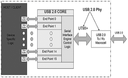
Figure 1. USB 2.0 PHY Integrated in SOC
The PHY is comprised of complex analog and digital macros to interface with the USB 2.0 and UTMI+ buses. PHY verification represents a typical challenge to achieve high quality IP in a small time-to-market; this is due to the need to verify the analog and digital parts separately and verifying the whole PHY in a mixed-signal environment. The following section shows the mixed-signal verification platform developed to verify the USB 2.0 PHY design [4].
3. USB 2.0 Mixed-Signal Verification
Verifying a mixed-signal IP is a more complex task than designing the IP, well defined verification plan is required in the early phases of the deign. The verification plan includes both simulation and modeling plans [5, 6]. Simulation plan includes the required test benches to ensure proper functionality of the analog and digital blocks and that the analog and digital macros are successfully integrated. The modeling plan is required to maximize the efficiency and enhance simulation speed, it determines which blocks require to be modeled and what effects to be included. The following subsections show the details of the implemented verification plan.
3.1. Analog Blocks Verification
The analog blocks are first verified on the transistor-level, each has a separate test bench, to check that it fulfills the specified functionality and performance defined by the analog specifications. Some blocks are selected to be verified using accurate analog simulator and other blocks are simulated using fast-spice simulator beside the analog simulator, in our verification flow we are using ELDOTM [7] as an accurate analog simulator and MACHTM [8] or ADITTM [9] as fast-spice simulators. The usage of fast-spice simulators is useful for speeding up the iterative simulations needed to optimize block performance, especially in feedback loops which require a long simulation time such as PLLs and CDRs. At the end of the block design cycle, the block is checked and optimized using analog simulator to guarantee accurate simulation results.
Besides verifying the required functionality, the analog blocks are also checked for their sensitivity for transistors mismatch, PVT corners, reliability and their functionality in the presence of bond wire, package and cable models.
For example, the HS transmitter is verified to cover the required functionality in the presence of the cable model with different lengths and check that the simulated eye-diagram passes the reference eye opening, the eye-diagram is also checked with the presence of supply variation to check the data coupled jitter effect. Another example is the verification of the PLL, where it is required to check its locking to 480MHz within the available locking period under all PVT corners. Also checking the output clock jitter and its sensitivity to supply variations is one of the important checks at PLL block verification. Also the verification of the CDR is very challenging as it should recovers the clock from the received data and guarantee a phase locking condition between the received data and the recovered clock at all process corners and for different data patterns.
3.2. Digital Blocks Verification
The Digital Part for the PHY is composed of two main data processing blocks, namely the transmission path and the reception path, in addition to other blocks either serving specific protocol functions to help the USB system detect events such as a bus disconnection, or providing power and clock management for the PHY which can operate in three speed modes (high speed, full speed or low speed). Verifying the digital Part of the PHY involves testing each of the main processing paths thoroughly, this involves the use of test vectors tailored to the USB/UTMI specifications and designed to test different design corners. Other UTMI specifications may require specific features within a test bench environment in order to test, among them are the minimum and maximum inter-packet delays for different operational speeds, as well as special operational modes which are used primarily for speed negotiation (Chirp).
Our verification approach for the PHY included the use of different testing platforms each having its own flavor in testing the main processing paths. The PHY is functionally verified on three levels, the first and most basic is done using deterministic data patterns for transmission and reception, where an automated testing platform exercises both reception and transmission paths and insures that the data patterns produced by the PHY during TX/RX comply with the UTMI standard. This stage of testing relies on testing patterns manually optimized to target specific data path corners within the PHY. Not all aspects of the system specifications are tested at this level, since the testing suite is optimized to deal with the more complex parts of the design which require the definition of specific vectors to test, this is particularly the case for the TX and RX paths which are vulnerable to many design corners that are generated by the way the UTMI is specified. Examples of specifications that contribute to hidden design corners include; stuffing operations, having different operational/speed modes for the PHY, and the frequency difference between the USB bus and the UTMI bus which has to be accommodated by the PHY.
The second stage of testing involves exercising the PHY using constrained random data patterns in order to check for any design corners missed in the first stage, the testing platform employed relies on the use of two PHYs connected in a back to back configuration where data patterns presented are transmitted by one PHY and received by the other, the integrity of the transfer operation is automatically checked. Thousands of packets generated pseudo-randomly using different constraints on data pattern structures are successfully transferred by the PHY at this stage, typically a verification run on ModelsimTM would take from few hours to several days depending on the number of packets to be tested. To insure the basic interoperability of the digital and analog parts of the PHY, the behavioral models for other analog parts of the PHY are employed. The use of monitors and checkers are also employed at this stage to keep an eye on the packet transactions at the USB bus level, this level is otherwise entirely not visible to the test bench. A USB Monitor package provided with Zero-In (a formal verification tool by Mentor Graphics) is utilized for this purpose.
Special considerations are also made during this second stage to insure compliance with different UTMI/USB devices that could introduce some distortions to the packets as they travel on the USB bus. A typical example is the presence of USB HUBs which may remove or add to parts of USB packets. For proper compliance with both standards (USB/UTMI) models are made to take into account those factors as well.
The third stage of testing is the system level, where the same back to back PHY configuration is used, however this time with two USB controllers; the controllers exercise the PHY in order to perform USB transactions specified by a top level system test bench which is written to verify the USB Controllers, of course while doing so it also exercises the PHYs to complete the transactions and uncovers any USB specifications incompatibility issues for the PHY, such issues may have remained uncovered until this stage since previous testing stages are more focused on the UTMI specifications than USB system level specifications.
3.3. Mixed-Level Verification
Besides verifying the analog and digital macros separately, mixed-level verification is needed to verify the analog and digital blocks in the context of the whole PHY system, in addition to checking the interface between the analog and digital macros. mixed-level verification using spice simulators requires long simulation times, whereas digital simulators can not deal with analog functions. The capability to freely mix and exchange different levels of abstraction; analog behavioral model, schematic or extracted netlist with parasitics, and digital block models, such as digital behavioral models, RTL or extracted gate level is a key for verifying mixed-signal designs [5,6]. ADVance MSTM [10] is used in our flow to simulate the system represented by these different views.
The mixed-level test benches were developed in order to cover verifying all the control signals from the digital macro to the analog blocks, in addition to verifying the modes and paths that require interaction between the analog and digital blocks. This is verified by selecting the appropriate views for the design blocks, as well as the required simulation accuracy by using either analog or fast spice simulators. As an example, the HS transmission was verified in order to check that the analog and digital blocks sharing this path are functioning properly. The path includes data serialization, bit stuffing and encoding in the digital part, the PLL clocking and the transmitter in the analog part. PLL and transmitter were selected as post-layout netlists, the digital part was represented in RTL. As the functionality of the transmitter depends on providing a good matching with the cable, so other blocks interacting with the data lines such as termination control and FS transmitter were partitioned to be simulated with fast spice simulator as the accuracy of simulating these blocks is not critical. All other blocks were selected as behavioral models.
Another critical path is the HS reception which receives and recovers the serial data and passes it to the digital part for deserialization, bit unstuffing and decoding. The timing relation between the signals of this path is critical and should be verified accurately. The path was verified using mixed-level simulations, the results are shown in Figure 2, where it shows the input analog serial data and the recovered data after it has been amplified by the receiver and recovered by the CDR. Also the output parallel data after deserialization in the digital part is shown, as well as the reception control signals which indicate if there is data activity on the lines and whether this data is valid or not and finally if there is an error in the received packet. Due to the critical timing issues in this path, the whole path was verified at the transistor-level including the analog and digital parts in order to check its proper functionality, this is done using fast-spice simulator to reduce simulation time.
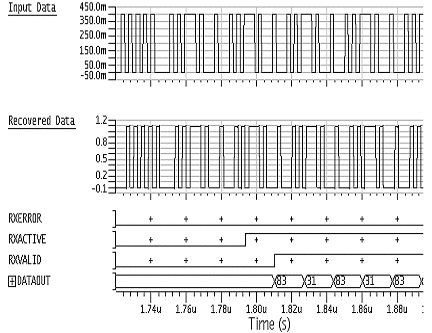
Figure 2. HS Reception Mixed-Level Simulation Results
To support the verification strategy, a robust test benches were developed and built for Scalability to support the reuse in different technologies, for Configurability such that all test benches variables are defined through parameters or generics in the main control file and for Automated Results Analysis to automatically extract the required results from the output waveforms and apply a predefined (Pass/Fail) criteria and reports the test run results.
The mixed-level test benches developed to exercise all the control signals and the shared functionalities between the analog and digital blocks are:
4. Conclusions
Robust mixed-signal verification methodology is required to greatly reduce the risk of chip failure and to achieve small time-to-market. This methodology relies on robust analog and digital verification flows, both combined into an upper level mixed-signal verification flow. This verification flow is successfully used in the design and implementation of the USB2.0 PHY IP.
5. Acknowledgments
We would like to thank the IP team in Mentor Graphics for its effort to establish the mixed-level verification flow for the USB2.0 PHY IP.
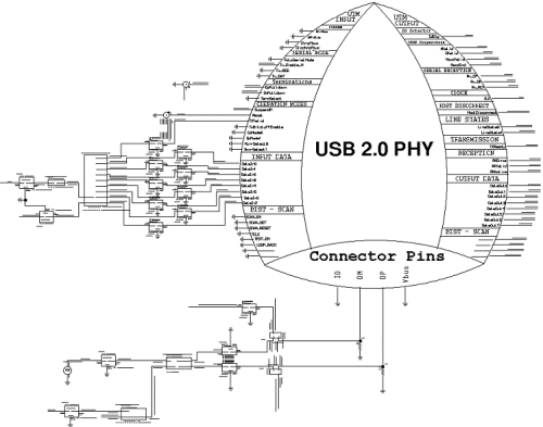
Figure 3. HS Transmission and Reception Mixed-Level Test Bench
6. References
[1] USB 2.0 Specification, July 16, 2007
[2] Intel Developer Forum 2007
[3] UTMI+ Specification, Revision 1.0, February 2, 2004.
[4] High-Speed USB 2.0 PHY Datasheet, Mentor Graphics.
[5] Ken Kundert. Principles of top-down mixed-signal design. , 2006.
[6] Ken Kundert and Henry Chang. Verification of complex analog integrated circuits. In IEEE 2006 Custom Integrated Circuits Conference (CICC), pages 177 – 184, 2006.
[7] ELDOTM User’s Manual, Mentor Graphics, v6.9 1, AMS 2007.1.
[8] Mach TATM User’s and Reference Manual, Mentor Graphics, v3.9 1, AMS 2007.1.
[9] ADiTTM User’s and Reference Manual, Mentor Graphics 2007.1.
[10] ADVance MSTM User’s Manual, Mentor Graphics, AMS 2007.1.
Abstract:
A well planned verification flow for a mixed-signal IP is required to achieve the highest quality of the IP performance with the expected design specifications. The aim of this paper is to present a mixed-signal verification flow for the Universal Serial Bus physical layer IP. The verification flow for both the analog and digital blocks in the USB2.0 PHY are presented. A combined mixed-signal system level verification flow for the whole IP is introduced. Examples for different test benches required to verify the USB2.0 PHY IP is presented with some illustration results.
1. Introduction
The increasing complexity of the end product electronics systems; put more challenges on the engineering design groups to meet shorter time-to-market with the highest required quality. Using Intellectual Property designs is one of the solutions that could help end-product designers to quickly integrate and assemble their complex systems using different IPs. However the main concern for system engineers is the quality of the IP and how good it will perform as expected within their systems. This makes IP verification one of the most challenging issues for IP designers. Considering the fact that the IP could be integrated into any unknown system or environment; this makes the scope of the IP verification plan wider and to consider any possible different scenarios for IP/System integration. One of the common used IPs in the market is the Universal Serial Bus IP. Since its release in 1995; the USB interface proves to be one of the most successful interfaces for serial data transfers. The first USB 1.x data transfer rates were at Low-Speed 1.5Mbps & Full-Speed 12Mbps. These data rates were good enough for low and medium speed applications such as computer peripherals and flash memory storage drives. The success of USB 1.x and the growing market demand for high speed data applications; paved the way for USB 2.0; released by the USB-IF in 2001 [1]. The High-Speed USB 2.0 data transfer rate is 480 Mbps. USB 2.0 is now a common port in almost all multimedia and portable applications such as portable MP3 players, digital cameras, video camcorders, gaming consoles and even TV sets now have a USB port. The growing expansion of the multimedia market will require higher data rate transfers for larger multimedia files. The Super-Speed USB 3.0 initial proposal are already out there with 10x faster than USB 2.0 and a data rate of 4.8Gbps [2].
Considering the USB physical layer; the USB PHY consists of both analog and digital blocks forming a mixed-mode signal IP. In this paper; a mixed-signal verification flow for the USB PHY IP is introduced. Although the paper is based on the mixed-signal verification of USB 2.0 physical layer (PHY), the same concepts can be used in other PHYs verification such as PCI-Express and SATA. Section 2 shows an overview on the USB interface, section 3 presents the mixed-signal verification flow including the analog and digital flows and covering the full integrated USB PHY IP mixed-level verification.
2. Universal Serial Bus Interface Overview
The Universal Serial Bus (USB) is a serial interface to allow connections to the PC without expansion cards. The USB 2.0 standard release supports High Speed (HS) traffic at 480Mbps while remaining backward compatible with USB 1.1 protocol, supporting the Full Speed (FS) traffic at 12Mbps and the Low- Speed (LS) traffic at 1.5Mbps.
Figure 1 shows the USB 2.0 system integrated in SOC ASIC device. The USB 2.0 PHY acts like a bridge. On one side it communicates to other USB compliant devices such as Host, Hub or Peripheral through a USB 2.0 bus. On the second side it communicates through the USB Transceiver Macrocell Interface (UTMI+) bus [3] to the USB 2.0 Core, or called the Serial Interface Engine (SIE), present in the SOC ASIC. The data through the USB 2.0 bus is communicating in serial, half-duplex mode, while the data through the UTMI+ bus is communicating in parallel selectable between 8 bits or 16 bits options.

Figure 1. USB 2.0 PHY Integrated in SOC
The PHY is comprised of complex analog and digital macros to interface with the USB 2.0 and UTMI+ buses. PHY verification represents a typical challenge to achieve high quality IP in a small time-to-market; this is due to the need to verify the analog and digital parts separately and verifying the whole PHY in a mixed-signal environment. The following section shows the mixed-signal verification platform developed to verify the USB 2.0 PHY design [4].
3. USB 2.0 Mixed-Signal Verification
Verifying a mixed-signal IP is a more complex task than designing the IP, well defined verification plan is required in the early phases of the deign. The verification plan includes both simulation and modeling plans [5, 6]. Simulation plan includes the required test benches to ensure proper functionality of the analog and digital blocks and that the analog and digital macros are successfully integrated. The modeling plan is required to maximize the efficiency and enhance simulation speed, it determines which blocks require to be modeled and what effects to be included. The following subsections show the details of the implemented verification plan.
3.1. Analog Blocks Verification
The analog blocks are first verified on the transistor-level, each has a separate test bench, to check that it fulfills the specified functionality and performance defined by the analog specifications. Some blocks are selected to be verified using accurate analog simulator and other blocks are simulated using fast-spice simulator beside the analog simulator, in our verification flow we are using ELDOTM [7] as an accurate analog simulator and MACHTM [8] or ADITTM [9] as fast-spice simulators. The usage of fast-spice simulators is useful for speeding up the iterative simulations needed to optimize block performance, especially in feedback loops which require a long simulation time such as PLLs and CDRs. At the end of the block design cycle, the block is checked and optimized using analog simulator to guarantee accurate simulation results.
Besides verifying the required functionality, the analog blocks are also checked for their sensitivity for transistors mismatch, PVT corners, reliability and their functionality in the presence of bond wire, package and cable models.
For example, the HS transmitter is verified to cover the required functionality in the presence of the cable model with different lengths and check that the simulated eye-diagram passes the reference eye opening, the eye-diagram is also checked with the presence of supply variation to check the data coupled jitter effect. Another example is the verification of the PLL, where it is required to check its locking to 480MHz within the available locking period under all PVT corners. Also checking the output clock jitter and its sensitivity to supply variations is one of the important checks at PLL block verification. Also the verification of the CDR is very challenging as it should recovers the clock from the received data and guarantee a phase locking condition between the received data and the recovered clock at all process corners and for different data patterns.
3.2. Digital Blocks Verification
The Digital Part for the PHY is composed of two main data processing blocks, namely the transmission path and the reception path, in addition to other blocks either serving specific protocol functions to help the USB system detect events such as a bus disconnection, or providing power and clock management for the PHY which can operate in three speed modes (high speed, full speed or low speed). Verifying the digital Part of the PHY involves testing each of the main processing paths thoroughly, this involves the use of test vectors tailored to the USB/UTMI specifications and designed to test different design corners. Other UTMI specifications may require specific features within a test bench environment in order to test, among them are the minimum and maximum inter-packet delays for different operational speeds, as well as special operational modes which are used primarily for speed negotiation (Chirp).
Our verification approach for the PHY included the use of different testing platforms each having its own flavor in testing the main processing paths. The PHY is functionally verified on three levels, the first and most basic is done using deterministic data patterns for transmission and reception, where an automated testing platform exercises both reception and transmission paths and insures that the data patterns produced by the PHY during TX/RX comply with the UTMI standard. This stage of testing relies on testing patterns manually optimized to target specific data path corners within the PHY. Not all aspects of the system specifications are tested at this level, since the testing suite is optimized to deal with the more complex parts of the design which require the definition of specific vectors to test, this is particularly the case for the TX and RX paths which are vulnerable to many design corners that are generated by the way the UTMI is specified. Examples of specifications that contribute to hidden design corners include; stuffing operations, having different operational/speed modes for the PHY, and the frequency difference between the USB bus and the UTMI bus which has to be accommodated by the PHY.
The second stage of testing involves exercising the PHY using constrained random data patterns in order to check for any design corners missed in the first stage, the testing platform employed relies on the use of two PHYs connected in a back to back configuration where data patterns presented are transmitted by one PHY and received by the other, the integrity of the transfer operation is automatically checked. Thousands of packets generated pseudo-randomly using different constraints on data pattern structures are successfully transferred by the PHY at this stage, typically a verification run on ModelsimTM would take from few hours to several days depending on the number of packets to be tested. To insure the basic interoperability of the digital and analog parts of the PHY, the behavioral models for other analog parts of the PHY are employed. The use of monitors and checkers are also employed at this stage to keep an eye on the packet transactions at the USB bus level, this level is otherwise entirely not visible to the test bench. A USB Monitor package provided with Zero-In (a formal verification tool by Mentor Graphics) is utilized for this purpose.
Special considerations are also made during this second stage to insure compliance with different UTMI/USB devices that could introduce some distortions to the packets as they travel on the USB bus. A typical example is the presence of USB HUBs which may remove or add to parts of USB packets. For proper compliance with both standards (USB/UTMI) models are made to take into account those factors as well.
The third stage of testing is the system level, where the same back to back PHY configuration is used, however this time with two USB controllers; the controllers exercise the PHY in order to perform USB transactions specified by a top level system test bench which is written to verify the USB Controllers, of course while doing so it also exercises the PHYs to complete the transactions and uncovers any USB specifications incompatibility issues for the PHY, such issues may have remained uncovered until this stage since previous testing stages are more focused on the UTMI specifications than USB system level specifications.
3.3. Mixed-Level Verification
Besides verifying the analog and digital macros separately, mixed-level verification is needed to verify the analog and digital blocks in the context of the whole PHY system, in addition to checking the interface between the analog and digital macros. mixed-level verification using spice simulators requires long simulation times, whereas digital simulators can not deal with analog functions. The capability to freely mix and exchange different levels of abstraction; analog behavioral model, schematic or extracted netlist with parasitics, and digital block models, such as digital behavioral models, RTL or extracted gate level is a key for verifying mixed-signal designs [5,6]. ADVance MSTM [10] is used in our flow to simulate the system represented by these different views.
The mixed-level test benches were developed in order to cover verifying all the control signals from the digital macro to the analog blocks, in addition to verifying the modes and paths that require interaction between the analog and digital blocks. This is verified by selecting the appropriate views for the design blocks, as well as the required simulation accuracy by using either analog or fast spice simulators. As an example, the HS transmission was verified in order to check that the analog and digital blocks sharing this path are functioning properly. The path includes data serialization, bit stuffing and encoding in the digital part, the PLL clocking and the transmitter in the analog part. PLL and transmitter were selected as post-layout netlists, the digital part was represented in RTL. As the functionality of the transmitter depends on providing a good matching with the cable, so other blocks interacting with the data lines such as termination control and FS transmitter were partitioned to be simulated with fast spice simulator as the accuracy of simulating these blocks is not critical. All other blocks were selected as behavioral models.
Another critical path is the HS reception which receives and recovers the serial data and passes it to the digital part for deserialization, bit unstuffing and decoding. The timing relation between the signals of this path is critical and should be verified accurately. The path was verified using mixed-level simulations, the results are shown in Figure 2, where it shows the input analog serial data and the recovered data after it has been amplified by the receiver and recovered by the CDR. Also the output parallel data after deserialization in the digital part is shown, as well as the reception control signals which indicate if there is data activity on the lines and whether this data is valid or not and finally if there is an error in the received packet. Due to the critical timing issues in this path, the whole path was verified at the transistor-level including the analog and digital parts in order to check its proper functionality, this is done using fast-spice simulator to reduce simulation time.

Figure 2. HS Reception Mixed-Level Simulation Results
To support the verification strategy, a robust test benches were developed and built for Scalability to support the reuse in different technologies, for Configurability such that all test benches variables are defined through parameters or generics in the main control file and for Automated Results Analysis to automatically extract the required results from the output waveforms and apply a predefined (Pass/Fail) criteria and reports the test run results.
The mixed-level test benches developed to exercise all the control signals and the shared functionalities between the analog and digital blocks are:
- High-speed transmission and reception
- Full-speed transmission and reception
- Low-speed transmission and reception
- Full-speed device disconnection
- High-speed device disconnection
- Serial mode transmission and reception
- Opmodes
- VBUS and ID operations
- IDDQ current
- Built In Self Test (BIST)
4. Conclusions
Robust mixed-signal verification methodology is required to greatly reduce the risk of chip failure and to achieve small time-to-market. This methodology relies on robust analog and digital verification flows, both combined into an upper level mixed-signal verification flow. This verification flow is successfully used in the design and implementation of the USB2.0 PHY IP.
5. Acknowledgments
We would like to thank the IP team in Mentor Graphics for its effort to establish the mixed-level verification flow for the USB2.0 PHY IP.

Figure 3. HS Transmission and Reception Mixed-Level Test Bench
6. References
[1] USB 2.0 Specification, July 16, 2007
[2] Intel Developer Forum 2007
[3] UTMI+ Specification, Revision 1.0, February 2, 2004.
[4] High-Speed USB 2.0 PHY Datasheet, Mentor Graphics.
[5] Ken Kundert. Principles of top-down mixed-signal design. , 2006.
[6] Ken Kundert and Henry Chang. Verification of complex analog integrated circuits. In IEEE 2006 Custom Integrated Circuits Conference (CICC), pages 177 – 184, 2006.
[7] ELDOTM User’s Manual, Mentor Graphics, v6.9 1, AMS 2007.1.
[8] Mach TATM User’s and Reference Manual, Mentor Graphics, v3.9 1, AMS 2007.1.
[9] ADiTTM User’s and Reference Manual, Mentor Graphics 2007.1.
[10] ADVance MSTM User’s Manual, Mentor Graphics, AMS 2007.1.
