By Bhaskarabhotla Leela Madhuri, He Mee Hing, Anjali Vishwanath
Infineon Technologies Asia Pacific Pte Ltd
Abstract
This paper briefly discusses the approaches for Validation Environment and Test methodologies adopted for 8-bit microcontroller family based products. We would be focusing on modularity and the need to adapt various test methodologies with the thought of reuse. The aim of this paper is to raise the awareness for specific advantages/disadvantages, the time saving features and also the amount of reuse facilitated by the approach.
1. Introduction
Product Family Roadmap gives a brief overview of the strategic development for the management, while for the validation team it helps to focus on reuse at a very initial phase.
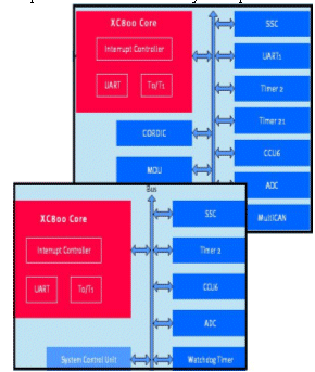
Fig 1. 8-bit derivatives overview
From Fig1 we can note that different derivative products have about ~80% reuse in terms of peripheral sets. We would be focusing on a 8-bit family which consists of XC800 core (Infineon 8-bit microcontroller’s core) and peripheral sets. It is important to understand the differences between different products at a very initial phase. The targeted validation environment should focus on the similarities for reuse and differences should be taken care, in order to facilitate the ease of reuse across the family of products.
2. Validation Environment
Validation environment refers to the complete set up to prove how it is being planned to evaluate the in-system requirements on the arrival of first silicon to track down hidden bugs which are uncovered by verification in the early stages of silicon analysis (pre-silicon verification, which mainly consists of RTL and gate-level simulations) in order to avoid massive failures before going for mass production.
The environment consists of validation testing methodologies, test benches set up, coverage analysis, problem/failure analysis and report tracking to ensure the silicon meets all the target specifications.
Validation environment set up frame work should be started in parallel with design activities once the specifications are available. Environment set up flow is consisted of the test case definitions, identify the reuse part with respect to verification, testing set up, common work area to store the data base, amount of coverage, standard libraries for commonality across the test cases.
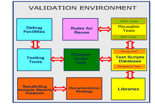
Fig 2. Overview of Validation Environment
From Fig2, the reusable components are separated from reusable and non-reusable components in order to facilitate early validation environment ramp up upon the arrival of product silicon.
Normally the challenges faced in post silicon validation are design complexity, signal integrity, power and thermal management which has to be addressed thoroughly in post silicon validation.
3. Necessity for Validation Against Pre-silicon Verification
Before we begin with validation approaches, it is necessary to understand why post-silicon validation is necessary. The ever increasing system-on-chip complexity, product time-to-market pressure and the automotive industry stringent requirements have led to a new approach in performing the validation activity at the post-silicon stage. The importance of the validation activities cannot be underestimated; as not all aspects of the verification can be covered within the pre-silicon stage. This means the following activities cannot be easily reproduced during RTL verification environment.
Here we will be focusing on the activities done on XC800 family product validation environment.
4. 1. Modularity
Since all products are based on the same XC800 core, we would be discussing below how to attain reuse with modularity. To certain extent, the scripts used for verification activities can be reused in validation stage. This can be realized if the verification activities are organized in a modular manner. Across the product family, common peripherals are used in multiple products with minor differences in the feature set. Chip verification scripts for such peripherals can be completely reused at validation stage, which saves development effort and time, while maintaining the consistency of both environments. A significant advantage of this approach is that the results can be correlated and cross-checked easily at any point of time of these two stages. On top of that, the same scripts can be used again across the product family. Minor adaptation might be needed, however the benefits that the approach outweighed the effort needed.
In cases where the validation environment is not shared with the verification environment, the test cases can still be shared in common with the validation environment in order to facilitate early setup and debug of flaws within the environment itself. Generally, the reusability of the scripts and common libraries between verification and validation environment can be categorized as followed:
1) 100% reusability – all functional aspects can be verified in the same manner in both verification and validation environment. Therefore, the functional verification scripts will not be changed between these two phases. Fig 3. Shows the seamless test scripts migration from verification to validation phase.
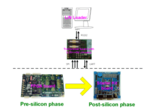
Fig 3. Environment for 100% reusability
2) 50% reusability – To some extent the database expertise or knowledge can be utilized during validation planning phase from verification. The environment is not completely reusable in this case and needs to be adapted for validation purpose.
3) 0% reusability – In this case, the validation and verification environment is totally different. This usually occurs when functional coverage is different under these two phases. System-level test can only be done in validation environment, e.g. system-level stress test which involves concurrent activities occurs in multiple peripherals, buses and memory spaces.
4.2. Coverage
Although pre-silicon verification gives an extensive amount of coverage which can be categorized as branch coverage, statement coverage, toggle coverage and functional coverage, there are still grey areas which can be covered only during validation phase, since validation addresses real-world scenario. Verification gives in-depth view of every signal transaction at the chip level, but the temperature variation cannot be simulated to certain extent. On the other hand, one will know how the device behaves in actual environment during validation although the occurrence of the actual signal may not be known. It is important to know the role of coverage in these two phases. Pre-silicon coverage plays a very important role since it is always better to find bugs at an earlier phase of design, but with the increasing complexity of today’s controllers it becomes extremely difficult to verify each and every function in the pre-silicon phase. The coverage in the pre-silicon phase is; module level verification the target for coverage is to achieve 100% line coverage and 100% of the defined functional coverage, while in SoC level the focus would be more on system level targets such as interconnectivity, etc. In validation phase (post-silicon verification) the coverage would be focusing on runtime behavior at different temperature zone and device performance under stress conditions. Thus verification and validation coverage goals compliment each other. One may argue that the weightage of coverage for pre-silicon phase should be on the higher side. It is true that pre-silicon verification is important as the quality of the chip would depend on it, even then we cannot neglect post-silicon validation. Post-silicon validation compliments pre-silicon verification where the focus is more on run-time issues and temperature variation testing etc.
5. Validation Test Methodologies
Validation consists of the environment and test methodologies. There are two main validation test methodologies:
5.1. Stress test
The coverage performed at verification stage may not be completed. Therefore, validation expands further the coverage which is not possible to be simulated in simulation environment. E.g. 100% RTL line coverage in simulation does not ensure the full functional coverage when it comes to system level integration. Based on this, stress test is introduced to complete the gap between these two stages.
In general, stress test can be briefly categorized into two areas: unit level stress test and system level stress test. Unit level stress test refers to stress condition performed on individual peripheral under extreme conditions, e.g. max & min functional values, electrical parameters and temperature over a period of time. At system level, more peripherals and internal bus systems are involved during the test. The focus is more towards validation of the expected behavior at system level, observation of the system behavior under boundary conditions, and also how the system behaves when it fails the stress test conditions.
For example, to test how a low-level driver performs under a stress environment cannot be realized in simulation. To perform the stress test at this level, the concept of dedicated resources and shared resources is introduced. The dedicated resource refers to the direct resource associated with the low-level driver, e.g. the dedicated resource of an SPI driver is the SPI peripheral. The shared resources refer to internal bus bandwidth, stack and memories.
The success of driver execution is based on the availability of dedicated resource and also the shared resources in a system. Dedicated resource is always available to the driver. When multiple low-level drivers are running in the device, all drivers will try to access to the limited shared resources available in the system. Unavailability of the shared resources will lead to the failure of the driver execution, which is the key idea behind the stress test concept. To do this, shared resources will be exhausted in a systematic manner while executing the low-level driver, and the system states are monitored closely until the system failed under certain scenarios. Once all of the driver failure criteria are met, all the necessary system parameters will be logged for further analysis. A significant benefit of this approach is that it reveals hidden problems which cannot be seen if unit-level regression test is performed.
To realize the above concept, a non-preemptive priority based scheduler is written to perform the tasks. Figure 4 below shows how the tasks are scheduled in the scheduler.
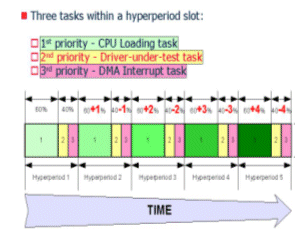
Fig 4. Scheduler of the system-level stress test
In this example, there are three tasks scheduled in the scheduler. These tasks will be executed in a dedicated timeframe known as hyperperiod, where the distribution of the shared resources among these tasks will be changed over time. As shown in the figure, the driver-under-test task, which is assigned as 2nd priority, will suffer from lack of shared resource over time and it will fail at certain point of time as the 1st priority task has consume most of the shared resources. The boundary condition will be repeated and observed, and the observation will be logged for further analysis. This can be a beneficial input for further improvement on the low-level driver and also the hardware design.
5. 2. Peripheral Validation
During product validation phase, the validation of peripherals cannot be ignored. Although the verification environment covers peripheral test to a greater extent, due to limitation of pre-silicon verification it needs to be addressed during the product validation phase.
Peripheral validation will also check the timing requirements as per specification. Functional validation of each peripheral needs to be done in order to check their integrity when the real device is available.
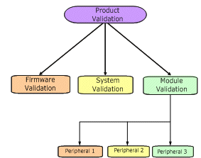
Fig 5. Peripheral validation
Peripheral validation can be subdivided in to in-system validation and peripherals validation. In-system validation will cover the features like firmware, System Control Unit (clock and reset), interrupt, debug interface, memories, etc. Peripheral validation covers the peripherals such as communication peripherals (SSC, CAN, SPI, etc), timers, A/D converters, etc.
Each individual peripheral will be tested for its completeness functionally against the given specification; which includes register checks, interface checks, interrupt checks, etc.
All the communication channels of the device with the external world will have to be tested thoroughly. Should check whether all the communication protocols supported are been met as per the standard specifications. If external memory interfaces are available they need to be validated too for the synchronization, data transfer speed, communicating with more than one external device in parallel.
The reuse component will be almost 100% in case of peripheral validation for family based products. There will be very minor differences among the respective peripherals across different products of a family.
Before planning reuse, it is necessary to take a deeper look into the architecture of the product with regard to individual peripheral. It is necessary to segregate the blocks where higher degree of reuse can be achieved against those where reuse is practically not possible.
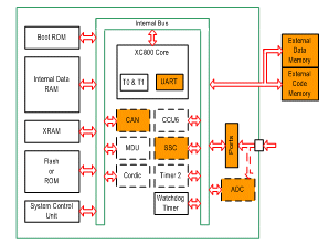
Fig 6. Typical Architecture of XC800 Family Microcontroller
Above figure depicts the generic architecture of XC800 Microcontroller family, the peripherals highlighted in the above picture [ADC, CAN, SSC, UART etc] will be almost same for most of the products in XC800 family. If planned in the early stages these common peripherals feature related validation tasks can be 100% reused across the family.
6. Rules for reuse
Following are some of the common rules or conventions that are followed to maintain the reusability of the test scripts:
Theoretically, 100% reuse can be achieved by following certain rules in a platform approach. Practically, we do not achieve complete reuse. Advance planning of product family between pre-silicon and post-silicon test environments minimizes the time required to find bugs in complex SoC designs and provides confidence that they are verified properly without side-effects.
The verification and validation community need to work together to share technologies and methods across product family domains, and bring in mutual benefits to productivity and efficiency.
8. Terminologies
Infineon Technologies Asia Pacific Pte Ltd
Abstract
This paper briefly discusses the approaches for Validation Environment and Test methodologies adopted for 8-bit microcontroller family based products. We would be focusing on modularity and the need to adapt various test methodologies with the thought of reuse. The aim of this paper is to raise the awareness for specific advantages/disadvantages, the time saving features and also the amount of reuse facilitated by the approach.
1. Introduction
Product Family Roadmap gives a brief overview of the strategic development for the management, while for the validation team it helps to focus on reuse at a very initial phase.

Fig 1. 8-bit derivatives overview
From Fig1 we can note that different derivative products have about ~80% reuse in terms of peripheral sets. We would be focusing on a 8-bit family which consists of XC800 core (Infineon 8-bit microcontroller’s core) and peripheral sets. It is important to understand the differences between different products at a very initial phase. The targeted validation environment should focus on the similarities for reuse and differences should be taken care, in order to facilitate the ease of reuse across the family of products.
2. Validation Environment
Validation environment refers to the complete set up to prove how it is being planned to evaluate the in-system requirements on the arrival of first silicon to track down hidden bugs which are uncovered by verification in the early stages of silicon analysis (pre-silicon verification, which mainly consists of RTL and gate-level simulations) in order to avoid massive failures before going for mass production.
The environment consists of validation testing methodologies, test benches set up, coverage analysis, problem/failure analysis and report tracking to ensure the silicon meets all the target specifications.
Validation environment set up frame work should be started in parallel with design activities once the specifications are available. Environment set up flow is consisted of the test case definitions, identify the reuse part with respect to verification, testing set up, common work area to store the data base, amount of coverage, standard libraries for commonality across the test cases.

Fig 2. Overview of Validation Environment
From Fig2, the reusable components are separated from reusable and non-reusable components in order to facilitate early validation environment ramp up upon the arrival of product silicon.
Normally the challenges faced in post silicon validation are design complexity, signal integrity, power and thermal management which has to be addressed thoroughly in post silicon validation.
3. Necessity for Validation Against Pre-silicon Verification
Before we begin with validation approaches, it is necessary to understand why post-silicon validation is necessary. The ever increasing system-on-chip complexity, product time-to-market pressure and the automotive industry stringent requirements have led to a new approach in performing the validation activity at the post-silicon stage. The importance of the validation activities cannot be underestimated; as not all aspects of the verification can be covered within the pre-silicon stage. This means the following activities cannot be easily reproduced during RTL verification environment.
-
Involve physical constraints; for example, temperature variation or electrical tests on the device
-
Involve system-level integration where some components are not ready at pre-silicon stage; for example, system-level stress test on the device where the test involves multiple peripherals transactions which increase over time
-
Combination of above; for example, running system-level stress test on the device at different temperature variation and verify if there is any flash data retention issues observed.
Here we will be focusing on the activities done on XC800 family product validation environment.
4. 1. Modularity
Since all products are based on the same XC800 core, we would be discussing below how to attain reuse with modularity. To certain extent, the scripts used for verification activities can be reused in validation stage. This can be realized if the verification activities are organized in a modular manner. Across the product family, common peripherals are used in multiple products with minor differences in the feature set. Chip verification scripts for such peripherals can be completely reused at validation stage, which saves development effort and time, while maintaining the consistency of both environments. A significant advantage of this approach is that the results can be correlated and cross-checked easily at any point of time of these two stages. On top of that, the same scripts can be used again across the product family. Minor adaptation might be needed, however the benefits that the approach outweighed the effort needed.
In cases where the validation environment is not shared with the verification environment, the test cases can still be shared in common with the validation environment in order to facilitate early setup and debug of flaws within the environment itself. Generally, the reusability of the scripts and common libraries between verification and validation environment can be categorized as followed:
1) 100% reusability – all functional aspects can be verified in the same manner in both verification and validation environment. Therefore, the functional verification scripts will not be changed between these two phases. Fig 3. Shows the seamless test scripts migration from verification to validation phase.

Fig 3. Environment for 100% reusability
2) 50% reusability – To some extent the database expertise or knowledge can be utilized during validation planning phase from verification. The environment is not completely reusable in this case and needs to be adapted for validation purpose.
3) 0% reusability – In this case, the validation and verification environment is totally different. This usually occurs when functional coverage is different under these two phases. System-level test can only be done in validation environment, e.g. system-level stress test which involves concurrent activities occurs in multiple peripherals, buses and memory spaces.
4.2. Coverage
Although pre-silicon verification gives an extensive amount of coverage which can be categorized as branch coverage, statement coverage, toggle coverage and functional coverage, there are still grey areas which can be covered only during validation phase, since validation addresses real-world scenario. Verification gives in-depth view of every signal transaction at the chip level, but the temperature variation cannot be simulated to certain extent. On the other hand, one will know how the device behaves in actual environment during validation although the occurrence of the actual signal may not be known. It is important to know the role of coverage in these two phases. Pre-silicon coverage plays a very important role since it is always better to find bugs at an earlier phase of design, but with the increasing complexity of today’s controllers it becomes extremely difficult to verify each and every function in the pre-silicon phase. The coverage in the pre-silicon phase is; module level verification the target for coverage is to achieve 100% line coverage and 100% of the defined functional coverage, while in SoC level the focus would be more on system level targets such as interconnectivity, etc. In validation phase (post-silicon verification) the coverage would be focusing on runtime behavior at different temperature zone and device performance under stress conditions. Thus verification and validation coverage goals compliment each other. One may argue that the weightage of coverage for pre-silicon phase should be on the higher side. It is true that pre-silicon verification is important as the quality of the chip would depend on it, even then we cannot neglect post-silicon validation. Post-silicon validation compliments pre-silicon verification where the focus is more on run-time issues and temperature variation testing etc.
5. Validation Test Methodologies
Validation consists of the environment and test methodologies. There are two main validation test methodologies:
5.1. Stress test
The coverage performed at verification stage may not be completed. Therefore, validation expands further the coverage which is not possible to be simulated in simulation environment. E.g. 100% RTL line coverage in simulation does not ensure the full functional coverage when it comes to system level integration. Based on this, stress test is introduced to complete the gap between these two stages.
In general, stress test can be briefly categorized into two areas: unit level stress test and system level stress test. Unit level stress test refers to stress condition performed on individual peripheral under extreme conditions, e.g. max & min functional values, electrical parameters and temperature over a period of time. At system level, more peripherals and internal bus systems are involved during the test. The focus is more towards validation of the expected behavior at system level, observation of the system behavior under boundary conditions, and also how the system behaves when it fails the stress test conditions.
For example, to test how a low-level driver performs under a stress environment cannot be realized in simulation. To perform the stress test at this level, the concept of dedicated resources and shared resources is introduced. The dedicated resource refers to the direct resource associated with the low-level driver, e.g. the dedicated resource of an SPI driver is the SPI peripheral. The shared resources refer to internal bus bandwidth, stack and memories.
The success of driver execution is based on the availability of dedicated resource and also the shared resources in a system. Dedicated resource is always available to the driver. When multiple low-level drivers are running in the device, all drivers will try to access to the limited shared resources available in the system. Unavailability of the shared resources will lead to the failure of the driver execution, which is the key idea behind the stress test concept. To do this, shared resources will be exhausted in a systematic manner while executing the low-level driver, and the system states are monitored closely until the system failed under certain scenarios. Once all of the driver failure criteria are met, all the necessary system parameters will be logged for further analysis. A significant benefit of this approach is that it reveals hidden problems which cannot be seen if unit-level regression test is performed.
To realize the above concept, a non-preemptive priority based scheduler is written to perform the tasks. Figure 4 below shows how the tasks are scheduled in the scheduler.

Fig 4. Scheduler of the system-level stress test
In this example, there are three tasks scheduled in the scheduler. These tasks will be executed in a dedicated timeframe known as hyperperiod, where the distribution of the shared resources among these tasks will be changed over time. As shown in the figure, the driver-under-test task, which is assigned as 2nd priority, will suffer from lack of shared resource over time and it will fail at certain point of time as the 1st priority task has consume most of the shared resources. The boundary condition will be repeated and observed, and the observation will be logged for further analysis. This can be a beneficial input for further improvement on the low-level driver and also the hardware design.
5. 2. Peripheral Validation
During product validation phase, the validation of peripherals cannot be ignored. Although the verification environment covers peripheral test to a greater extent, due to limitation of pre-silicon verification it needs to be addressed during the product validation phase.
Peripheral validation will also check the timing requirements as per specification. Functional validation of each peripheral needs to be done in order to check their integrity when the real device is available.

Fig 5. Peripheral validation
Peripheral validation can be subdivided in to in-system validation and peripherals validation. In-system validation will cover the features like firmware, System Control Unit (clock and reset), interrupt, debug interface, memories, etc. Peripheral validation covers the peripherals such as communication peripherals (SSC, CAN, SPI, etc), timers, A/D converters, etc.
Each individual peripheral will be tested for its completeness functionally against the given specification; which includes register checks, interface checks, interrupt checks, etc.
All the communication channels of the device with the external world will have to be tested thoroughly. Should check whether all the communication protocols supported are been met as per the standard specifications. If external memory interfaces are available they need to be validated too for the synchronization, data transfer speed, communicating with more than one external device in parallel.
The reuse component will be almost 100% in case of peripheral validation for family based products. There will be very minor differences among the respective peripherals across different products of a family.
Before planning reuse, it is necessary to take a deeper look into the architecture of the product with regard to individual peripheral. It is necessary to segregate the blocks where higher degree of reuse can be achieved against those where reuse is practically not possible.

Fig 6. Typical Architecture of XC800 Family Microcontroller
Above figure depicts the generic architecture of XC800 Microcontroller family, the peripherals highlighted in the above picture [ADC, CAN, SSC, UART etc] will be almost same for most of the products in XC800 family. If planned in the early stages these common peripherals feature related validation tasks can be 100% reused across the family.
6. Rules for reuse
Following are some of the common rules or conventions that are followed to maintain the reusability of the test scripts:
- Common template to be followed for the test scripts
- Function names to be maintained with common conventions
- Common libraries across the product family in order to increase the reuse amount
- Common work space and tool chain to be used for all the products in order to make the test scripts portable/compatible
- Central Database maintenance where the test scripts are stored for easier retrieval.
- Common platform to share the issues/problems/bugs found and the fixes worked out during validation phase
- Regular updates/communication among the validation group in order to maintain the latest info across various sites.
- Maintaining same product initial settings across the validation environment.
- Output format should be maintained in same manner
- Result logging of module test, start time, end time, run time, test results, etc are required for future analysis in case of issues found later.
- Reports of individual peripheral test for review by the developer.
Theoretically, 100% reuse can be achieved by following certain rules in a platform approach. Practically, we do not achieve complete reuse. Advance planning of product family between pre-silicon and post-silicon test environments minimizes the time required to find bugs in complex SoC designs and provides confidence that they are verified properly without side-effects.
The verification and validation community need to work together to share technologies and methods across product family domains, and bring in mutual benefits to productivity and efficiency.
8. Terminologies
- XC800 – 8-bit Microcontroller Family
- RTL – Register Transfer Level
- SSC – Synchronous Serial Interface
- CAN – Control Area Network
- SPI – Serial Peripheral Interface
- A/D – Analog to Digital
- UART–Universal Asynchronous Receiver/Transmitter
- ADC – Analog to Digital Converter
- SoC - System on Chip
