ST Microelectronics Pvt. Ltd.
Greater Noida, India
Abstract:
The complexity of today's SOC has increased many folds and in past few years new methodologies have been developed to model and design these complex chips. Transaction level modelling is one such methodology which allows system architects and verification engineers to work at a higher level of abstraction . These models can be developed as soon as initial functional specifications of SOCs are designed and can be helpful in many phases of design cycle like architecture models for HW/SW partitioning evaluations, reference models for functional verification and virtual prototype for developing and verifying their firmware at early stages of SOC development while hardware is under development and not fully verified.
For image signal processor SOCs, this methodology has been used for firmware development. However, it is almost impossible to work on the image quality and verify the close loop algorithms such as auto exposure, auto white balance and auto focus using these models as there is close interaction between the sensor and ISP.
In this paper, we discuss the Transaction Level Model which is being developed to act as Virtual Prototype in digital image processors designed to fit into mobile applications. As part of our developments new methodology TLMdevice is also defined which provides way to connect TLM simulations to communicate with not only virtual host devices such as Graphical window, Keyboards but also real host devices like UART, Display and Sensors, so that data can be easily sent and received to/from during TLM simulation run. The TLM models were interfaced with the SMIA complaint CMOS sensor using USB interface. Drivers were developed to configure sensor, capture the image from sensor and provide it to the SystemC TLM model.
Introduction:
A System on a chip comprises processors, timers, interrupt controllers, buses, memories and all along that a piece of embedded software; which is embedded in a hardware device and enables all of these to work. It acts as an operating system for the complete SOC.
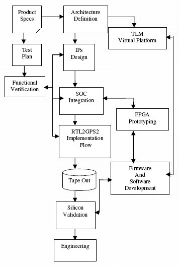
The traditional flow for any System-on-a-chip is:
- Architecture Definition, and Algorithms development using C or MatLab
- IPs design
- SOC Integration
- Functional Verification
- Physical Implementation
- FPGA Prototyping
- Firmware and SW Development
- Silicon Validation and Engineering.
At Imaging with each new project and new developments current design flow focuses first on RTL implementation and verification. It takes nearly 70% of total project duration to validate RTL for the device and FPGA prototype board cannot be made available unless RTL is mature enough. Firmware team is very much dependent upon FPGA prototype board for their developments to get started because of slow simulation speed on RTL simulation environments. Missing HW/SW codevelopment puts lot of pressure on firmware team and delay overall project design cycle. Even if firmware team validates their firmware on FPGA prototype board, they are unable to validate it against real scenarios for some specific close loop algorithms. Register specifications are primary input for firmware team; they may change during RTL implementation, thus delays firmware early developments and analysis.
Looking at the said challenges our aim was two fold, one was to help firmware team to start their developments early in the design cycle and second was to provide a platform which can plug-in with our existing functional verification environment and help verification engineers to have close loop bit true verification of complete SOC.
The diagram below shows the links between the main development phases and where the TLM Virtual Platform comes into the picture.

Figure 1: Silicon Development Phases
TLM is System Design Methodology which can be used to overcome these challenges. These TLM models are not as detailed, nor are they concerned with the micro architecture like RTL models. Rather, they correspond to the architecture level of abstraction. In this context, the term transaction refers to the exchange of a data or an event between two components of a modeled and simulated system. A data transaction can be a single word, a series of words or a complex data structure that is transferred over a bus between system components.
The philosophy behind these TLM models is to describe functionality in sufficient detail for the software team to start their analysis and firmware validation much earlier than using FPGA prototype.
Platform is made by integrating block (IPs) SystemC TLM model and TLM wrapper of ISS processor. Each IP is written in SystemC, or has at least a SystemC wrapper with its bit true C Model plugged inside which eases functional verification engineer’s job to verify SOC by just comparing images from TLM model and RTL.
Along with that it provides more benefits to the firmware developers:
-
SystemC TLM models can be made available as early as functional specification of IP is available, thus reducing overall project cycle duration.
-
Just executing a script, changes in register specs can be easily integrated in existing TLM models.
-
Simulation speed plays critical role in firmware development cycle. With SystemC TLM Models we can achieve simulation speed comparable to FPGA prototype platforms which makes them highly useful for firmware team.
-
ISS TLM wrapper is embedded with its own debugger, so firmware code can be easily debugged while in development phase.
-
TLMdevice methodology enables firmware code to be validated against real scenarios because of its ability to control real sensor registers and close loop algorithms validations.
-
Intermediate Images can be dumped using these models which enable firmware developer to know performance of the system in real manner.
All these benefits of SystemC TLM ease HW/SW co development, fill the gap in SOC functional verification and thus shorten overall project cycle.
Image Signal Processor TLM: An example SystemC TLM Model:
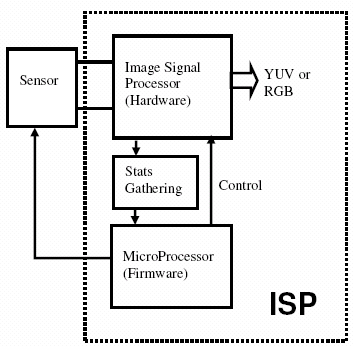
The task of Image Signal Processor (ISP) is to process the data into good quality image conforming to a standard format (YUV or RGB) after streaming bayer data from sensor.
It contains IPs for sensor defect correction, noise removal, bayer to rgb conversion and converting image data to YUV or RGB format according to output format expected by device. Different Statistics IPs gather stat information from input image like auto focus, auto exposure, white balancing etc which are being used by Firmware for image quality enhancement.
The SOC Level SystemC TLM is developed by Imaging STMicroelectronics to act as virtual prototype for Firmware development. TLMdevice server-client methodology internally developed by ST enables integration of real CMOS sensor with TLM model for real time verification of image processing firmware. TLMdevice is a set of libraries and programs to communicate between CMOS sensor & TLM platform and process live streamed images from sensor. The connection is based on socket communication to enable TLMdevice servers to be located any where on the network. The only tools required to develop such TLM IPs are the freeof- charge open source SystemC 2.0 kernel, C++, GNU compiler & gdb debugger.

Figure 2: Image Signal Processor Intellectual Property Block Diagram
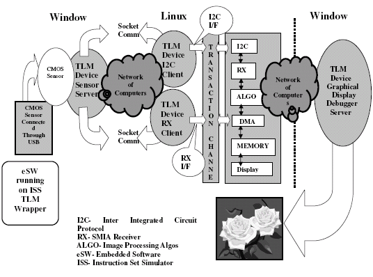
The developed SystemC TLM platform is composed of:
-
TLM wrapper of Instruction Set Simulator (ISS) Model of Micro Processor
-
TLMdevice Sensor Application (Interface for connecting HW CMOS Sensor with ISP TLM Platform)
-
SystemC TLM wrapper of Image Processing Algorithm IPs like sensor defect removal, noise removal, colour interpolation and output formatter with their bit true C models plugged inside.
-
SystemC TLM wrapper of Image Statistics Algorithm IPs with bit true C model plugged inside.
-
SystemC TLM Models of I2C, SMIA Receiver, Interrupt Controller, DMA and Memory.
-
TLMdevice Graphical Display Device (Interface for RGB/YUV image coming from ISP TLM platform for displaying on connected machine)
Internal Architecture of the Platform:
1. Following APIs have been implemented for TLM device communication:
- int Get_Image_Data (const char * image_data_ptr, int_32* size)
- void Read_Sensor_Register (int_32 address, int_32 * data)
- void Write_Sensor_Register (int_32 address, int_32 data)
- void Send_Image_Data (const char * image_data_ptr, int_32 size)
2. Transaction Accurate Channel is instantiated in the platform as follows:
- TAC_CHANNEL = new tac_router< GLOBAL_ADDRESS_TYPE, GLOBAL_DATA_TYPE > ("TAC_CHANNEL", "ADDRESS_MAP");
Data type is used to make implementation according to user defined implementation of channel for his needs.
3. Each Block is modeled as a SystemC Module, instantiated in the main function and connected through TAC Channel
- MASTER = new tac_Cpu_iss_wrapper <tlm_uint32_t,tlm_uint32_t> ("Cpu_api", embedded_software_path, debugger string, 100);
- ISP_INST = new isp("ISP_ INST");
- RX =new rx (“RXâ€);
- DISPLAY = new display (“DISPLAYâ€);
- I2C = new i2c (“I2C_SENSOR_COMMâ€);
- MEMORY= new memory(“MEMORYâ€,MEMSIZE,MEMB ASE);
- DMA = new dma (“DMAâ€);
- MASTER->initiator_port (TAC_CHANNEL->target_port);
- TAC_CHANNEL->initiator_port (ISP_INST->target_port);
- TAC_CHANNEL->initiator_port (RX->target_port);
- TAC_CHANNEL->initiator_port (I2C->target_port);
- TAC_CHANNEL->initiator_port (DMA->target_port);
- TAC_CHANNEL->initiator_port (MEMORY->target_port);
- TAC_CHANNEL->initiator_port (DISPLAY->target_port);
4. Similarly Other IPs can be connected. Below is couple of commands which are being used for read/write primitives:
- MASTER->initiator_port.write (ADDR, DATA);
5. Read a Block of data from Memory
- DMA.read (addr,BLOCK_SIZE);

Figure 3: Image Signal Processor TLM Model Block Diagram
Data Flow of the platform:
1. Embedded software running on ISS starts programming CMOS sensor using TLMdevice Sensor Application and other hardware TLM models.
2. The client side of TLMdevice uses 2 separate protocols for I2C and Receiver IP Interface
- TLMdevice Client/ I2C: This interface connects with I2C IP of TLM Platform and program sensor registers.
- TLMdevice Client/ Receiver: This interface connects with Receiver IP of TLM platform and send/receive RAW Bayer image data from the sensor.
3. The TLMdevice sensor server captures the raw data from CMOS sensor using MFCs APIs, and sends this data to TLMdevice client attached to TLM model of Receiver.
4. Once RAW Bayer Image is received by Receiver TLM platform, it extracts frame information from it, update size related hardware registers and send this image to Image Signal Processor IP of TLM Platform for further processing. ISP TLM model calls internally Bit true C Models of image processing algorithms to process image.
5. Different Intermediate images are stored in memory through DMA for debugging purposes.
6. The output image data from ISP is either in RGB or YUV format. TLMdevice Graphical Display Device client packs incoming data in appropriate data structures and sends this data to connected machine where TLMdevice Server is running for displaying.
7. To debug the embedded software, ISS debugger is used and there is a facility to record channel transactions also which can be viewed waveform viewer.
Results:
Using this SystemC TLM platform and TLMdevice Methodology significant time gain has been done for the Embedded Software development. Communication TLM platform with Real CMOS sensor enables firmware developers to validate real time algorithms on images directly streamed from sensor and upto 2 fps frame rate is achieved which made it highly useful for them. Socket programming between TLMdevice server and client, enables servers to be located anywhere on the network. ISS debugger made debugging easy for firmware developers.
Integration of Bit true C Model inside each IP TLM wrapper, proved this platform golden reference against RTL simulations for functional verification engineers. Image comparison between RTL and TLM Model made our verification flow fully automatic and 100% bit accurate.
Conclusion:
System Designers and embedded software developers are accepting that SystemC Transaction level models play a key role in different phases of SOC design cycle because of its many folds benefits like architecture models, golden reference models for functional verification, early availability to act as Virtual Prototype for image quality analysis and close loop validations.
This is the first level towards achieving significant reduction in time for embedded software development and OOPS concepts behind these TLM Models make them reusable for building a library of hardware and software components across many platforms which will ultimately reduce time to market for coming SOCs without sacrificing quality for hardware as well as embedded software.
Acknowledgments:
I would like to thank Mr. Giuseppe Bonanno for his cooperation in the area of TLM activities done in Imaging Group, ST Microelectronics Pvt Ltd.
Special Thanks to Mr. Mahesh Chandra, Project Manager at Imaging ST Microelectronics for providing me this opportunity and a word of Thanks to System Platforms Group in ST Microelectronics who have developed SystemC TLM Infrastructure globally to support other groups in their SOC TLM developments.
References:
-
Functional Specification of SystemC 2.0
-
Frank Vahid, Tony Givargis. “Embedded SystemC Design: A Unified Hardware/Software Introductionâ€. John Wiley & Sons,Inc
-
Transaction based methodology supports HW/SW co verification http://www.eetimes.com/story/OEG20030228S0061
-
SMIA Specifications
Author Biographs:
Mamta Chalana is a senior software engineer at STMicroelectronics, where she is working on SystemC TLM developments for Imaging Specific projects.
Naveen Khajuria is a senior software engineer at STMicroelectronics, working on SystemC TLM developments as a team member in System Platform Group.
