By Sameer Patel, Senior Director, Marketing
Atrenta Inc.
Systems and semiconductor suppliers are increasingly looking at methodology changes that can help accelerate assembly of chips and systems through one or multiple forms of automation. Why?
Over the past few years, the consumer revolution has led to a convergence of applications on a single device. The biggest example is the “ Smartphone†– handheld devices such as the iPhone or the BlackBerry that can enable consumers to read e-mail, text friends, create spreadsheets and documents, watch YouTube, play video games, listen to music, take pictures, store them, get directions, and yes, also make phone calls.
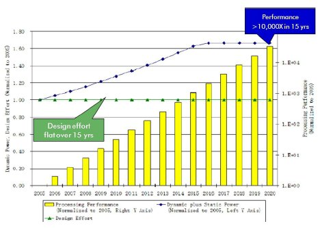
This convergence has resulted in increasing demands on design complexity and design performance. The ITRS organization estimates that design performance will grow over 10,000 times during the next 15 years (see Figure 1).

Figure 1: ITRS projections for performance and design effort growth
At the same time, due to a tighter economic climate as well as an increasingly competitive global marketplace, design teams are required to maintain (or even downsize) their current staffing levels. Effectively, they are being asked to deliver more with the same or fewer resources than before. The only way they can make this happen is by boosting the productivity of their design teams significantly.
The cost of a new design start at 45nm or below is now approaching (or will even exceed) $50M. Given this R&D investment in a single chip design start, the semiconductor supplier undertaking this design start would need to sustain a significant percentage of a $500M+ market for the return on investment (ROI) on that chip to make sense . The key question is how many such killer applications exist out there (besides the iPod or the iPhone) that can boast such a market size?
These trends point to the fact that semiconductor suppliers will need to start looking at alternative design techniques, such as platform-based design and IP reuse, to drive down the cost of design starts and more importantly, amortize these costs over several applications (or generations thereof) in order to get the desired ROI on their initial investment.
Finally, a major challenge facing all semiconductor suppliers today is shrinking market windows due to shorter product shelf lives. This means that it has become doubly important to ensure that designs hit the market as early as possible within the target market window in order to maximize the revenues from that design. Being late within the market window can have dire consequences, leading to a significant loss of potential revenue, or in some cases, a total loss of the market opportunity.
Given these trends, system and semiconductor suppliers are increasingly looking at methodology changes that can help accelerate assembly of chips and systems through one or multiple forms of automation.
Approaches to the problem
Let’s talk first about the technical challenges that SoC designers face today and then we will look at the potential solutions.
A modern SoC may contain 500 or more IPs (including integration logic), many of which may have 100 or more ports. Designers have already realized that creating, reviewing and maintaining 50,000 connections in a high level design language (HDL) through a text editor would be exceptionally painful. Many have moved to an eminently logical solution: capture the connections in a spreadsheet (e.g., Excel), then write a Perl script (or some form of script) to convert from that spreadsheet to a Verilog or VHDL netlist. However, spreadsheet-based solutions have a limitation in that they do not scale well across the needs of multiple design groups and business units within an organization.
SoC assembly tools support architectural level chip assembly and provide a rich set of capabilities to plan/edit a design, automate its assembly and establish feasibility. These solutions help reduce manual connectivity to the greatest degree possible and, in the process, provide a significant boost to design productivity. Designs are generated by adding instances in the design & making connections between them.
Building connectivity at RTL has its liabilities, the primary one being that users cannot use interfaces and interface connections. However, in order to manage complexity, designers absolutely need to be able to do so with minimal manual connectivity effort. Since each interface encapsulates a significant number of signals (for example an AXI bus), making connections through interfaces reduces the total number of connections by as much as 95%. Achieving this goal depends on heavy use of interfaces, rather than ad-hoc ports on components.

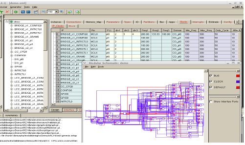
Figure 2: Defining architecture tables that drive automatic connectivity generation and viewing resulting schematics
Another trend in recent years has been to auto-generate major sub-systems of a system on chip (SoC) design. Few design teams would expect to have to build a bus fabric, a bridge or a clock subsystem by hand. At least one IP team within a company will build and maintain such generators – for proprietary bus fabrics, clock sub-systems and possibly other major sub-systems. Some companies use bus fabric generators from companies like ARM and Sonics. These provide multiple advantages – well proven software and quality of results, performance evaluation tools to help design optimal bus structures, and multiple forms of collateral data, including documentation, test-benches and timing constraints.
The same principle of fabric generators can be extended to other major sub-systems in a design, such as interrupt control, reset, configuration logic, memory sub-system, I/O, test and debug, and possibly other sub-systems also. The challenge is to combine automation with flexibility. Sub-system architectures do change over time and, to some extent, between significantly different applications. For example, you might not use the same clock generator for a standard application and a low power application.
In a true platform-based design, you can standardize the architecture for each integration logic sub-system such as bus, clock, reset, interrupt, power management, test, I/O, etc. What drives these decisions is how many of these subsystems can be built automatically using generators and high-level input for architectural choices. This approach eliminates the weeks of effort to implement these sub-systems in RTL. Engineering change orders (ECOs) can also be handled very easily and the fixes can be generated very quickly.
In almost any bus-centric design, software access to peripherals and data processing units is typically done through memory-mapped registers and memory blocks contained in (or accessed independently by) those IPs. Address offsets as seen from the host CPU are implemented through address translation logic in the various bus switches. Software development must largely proceed concurrently with hardware development even though the design may contain thousands of registers and hundreds of address maps.
This situation creates the need for very tightly controlled definitions of register and memory block locations, sizes and other characteristics in each IP, and equally for address map choices. As the design evolves and IP and address map requirements change, driven either from hardware or software development, it is critically important to be able to transparently reconcile such changes between the two teams. In most cases, the register/address map definition is built separately and concurrently with the design definition. However, users would benefit greatly from a methodology that reconciles the register/address map view back into the design view.
Customer results
Adoption of a structured SoC assembly methodology provides significant productivity boosts to SoC design teams. For example, one Atrenta customer, using 1Team®-Genesis, invested in defining interfaces for most major data and control functions, and also invested in developing generators for many of the architectural sub-systems. The first platform design took over 1 year to develop, as these models and generators were concurrently developed. The first derivative of that design, a fairly significant re-design but based on the same platform, was completed (to RTL handoff) in one month by one engineer.
In another instance, a customer used 1Team-Genesis for designing a wireless sub-system with 20 different IPs, 55 different instantiations and 12 RTL hierarchies. Using automated connectivity generation, this customer was able to define and generate the entire sub-system connectivity (170,000 lines of RTL code) in a couple of weeks as compared to the 3 months it took them with a manual connectivity approach.
Conclusion
Automated SoC assembly techniques have rapidly emerged as the standard approach for building today’s complex SoC designs. These solutions are enabling design teams to boost their productivity while lowering development costs. At the same time, these advanced approaches are helping them meet the stringent time-to-market requirements in today’s competitive global economy.
Sameer Patel is Senior Director, Marketing at Atrenta Inc. He has more than 19 years experience in the design and EDA industries and brings a strong processor design background to influence product direction for the architectural planning and feasibility solutions from Atrenta. Patel holds an MBA from UC Berkeley and a Master of Science Degree in Electrical Engineering from Virginia Tech.
Atrenta Inc.
Systems and semiconductor suppliers are increasingly looking at methodology changes that can help accelerate assembly of chips and systems through one or multiple forms of automation. Why?
Over the past few years, the consumer revolution has led to a convergence of applications on a single device. The biggest example is the “ Smartphone†– handheld devices such as the iPhone or the BlackBerry that can enable consumers to read e-mail, text friends, create spreadsheets and documents, watch YouTube, play video games, listen to music, take pictures, store them, get directions, and yes, also make phone calls.
This convergence has resulted in increasing demands on design complexity and design performance. The ITRS organization estimates that design performance will grow over 10,000 times during the next 15 years (see Figure 1).

Figure 1: ITRS projections for performance and design effort growth
At the same time, due to a tighter economic climate as well as an increasingly competitive global marketplace, design teams are required to maintain (or even downsize) their current staffing levels. Effectively, they are being asked to deliver more with the same or fewer resources than before. The only way they can make this happen is by boosting the productivity of their design teams significantly.
The cost of a new design start at 45nm or below is now approaching (or will even exceed) $50M. Given this R&D investment in a single chip design start, the semiconductor supplier undertaking this design start would need to sustain a significant percentage of a $500M+ market for the return on investment (ROI) on that chip to make sense . The key question is how many such killer applications exist out there (besides the iPod or the iPhone) that can boast such a market size?
These trends point to the fact that semiconductor suppliers will need to start looking at alternative design techniques, such as platform-based design and IP reuse, to drive down the cost of design starts and more importantly, amortize these costs over several applications (or generations thereof) in order to get the desired ROI on their initial investment.
Finally, a major challenge facing all semiconductor suppliers today is shrinking market windows due to shorter product shelf lives. This means that it has become doubly important to ensure that designs hit the market as early as possible within the target market window in order to maximize the revenues from that design. Being late within the market window can have dire consequences, leading to a significant loss of potential revenue, or in some cases, a total loss of the market opportunity.
Given these trends, system and semiconductor suppliers are increasingly looking at methodology changes that can help accelerate assembly of chips and systems through one or multiple forms of automation.
Approaches to the problem
Let’s talk first about the technical challenges that SoC designers face today and then we will look at the potential solutions.
A modern SoC may contain 500 or more IPs (including integration logic), many of which may have 100 or more ports. Designers have already realized that creating, reviewing and maintaining 50,000 connections in a high level design language (HDL) through a text editor would be exceptionally painful. Many have moved to an eminently logical solution: capture the connections in a spreadsheet (e.g., Excel), then write a Perl script (or some form of script) to convert from that spreadsheet to a Verilog or VHDL netlist. However, spreadsheet-based solutions have a limitation in that they do not scale well across the needs of multiple design groups and business units within an organization.
SoC assembly tools support architectural level chip assembly and provide a rich set of capabilities to plan/edit a design, automate its assembly and establish feasibility. These solutions help reduce manual connectivity to the greatest degree possible and, in the process, provide a significant boost to design productivity. Designs are generated by adding instances in the design & making connections between them.
Building connectivity at RTL has its liabilities, the primary one being that users cannot use interfaces and interface connections. However, in order to manage complexity, designers absolutely need to be able to do so with minimal manual connectivity effort. Since each interface encapsulates a significant number of signals (for example an AXI bus), making connections through interfaces reduces the total number of connections by as much as 95%. Achieving this goal depends on heavy use of interfaces, rather than ad-hoc ports on components.

Figure 2: Defining architecture tables that drive automatic connectivity generation and viewing resulting schematics
Another trend in recent years has been to auto-generate major sub-systems of a system on chip (SoC) design. Few design teams would expect to have to build a bus fabric, a bridge or a clock subsystem by hand. At least one IP team within a company will build and maintain such generators – for proprietary bus fabrics, clock sub-systems and possibly other major sub-systems. Some companies use bus fabric generators from companies like ARM and Sonics. These provide multiple advantages – well proven software and quality of results, performance evaluation tools to help design optimal bus structures, and multiple forms of collateral data, including documentation, test-benches and timing constraints.
The same principle of fabric generators can be extended to other major sub-systems in a design, such as interrupt control, reset, configuration logic, memory sub-system, I/O, test and debug, and possibly other sub-systems also. The challenge is to combine automation with flexibility. Sub-system architectures do change over time and, to some extent, between significantly different applications. For example, you might not use the same clock generator for a standard application and a low power application.
In a true platform-based design, you can standardize the architecture for each integration logic sub-system such as bus, clock, reset, interrupt, power management, test, I/O, etc. What drives these decisions is how many of these subsystems can be built automatically using generators and high-level input for architectural choices. This approach eliminates the weeks of effort to implement these sub-systems in RTL. Engineering change orders (ECOs) can also be handled very easily and the fixes can be generated very quickly.
In almost any bus-centric design, software access to peripherals and data processing units is typically done through memory-mapped registers and memory blocks contained in (or accessed independently by) those IPs. Address offsets as seen from the host CPU are implemented through address translation logic in the various bus switches. Software development must largely proceed concurrently with hardware development even though the design may contain thousands of registers and hundreds of address maps.
This situation creates the need for very tightly controlled definitions of register and memory block locations, sizes and other characteristics in each IP, and equally for address map choices. As the design evolves and IP and address map requirements change, driven either from hardware or software development, it is critically important to be able to transparently reconcile such changes between the two teams. In most cases, the register/address map definition is built separately and concurrently with the design definition. However, users would benefit greatly from a methodology that reconciles the register/address map view back into the design view.
Customer results
Adoption of a structured SoC assembly methodology provides significant productivity boosts to SoC design teams. For example, one Atrenta customer, using 1Team®-Genesis, invested in defining interfaces for most major data and control functions, and also invested in developing generators for many of the architectural sub-systems. The first platform design took over 1 year to develop, as these models and generators were concurrently developed. The first derivative of that design, a fairly significant re-design but based on the same platform, was completed (to RTL handoff) in one month by one engineer.
In another instance, a customer used 1Team-Genesis for designing a wireless sub-system with 20 different IPs, 55 different instantiations and 12 RTL hierarchies. Using automated connectivity generation, this customer was able to define and generate the entire sub-system connectivity (170,000 lines of RTL code) in a couple of weeks as compared to the 3 months it took them with a manual connectivity approach.
Conclusion
Automated SoC assembly techniques have rapidly emerged as the standard approach for building today’s complex SoC designs. These solutions are enabling design teams to boost their productivity while lowering development costs. At the same time, these advanced approaches are helping them meet the stringent time-to-market requirements in today’s competitive global economy.
Sameer Patel is Senior Director, Marketing at Atrenta Inc. He has more than 19 years experience in the design and EDA industries and brings a strong processor design background to influence product direction for the architectural planning and feasibility solutions from Atrenta. Patel holds an MBA from UC Berkeley and a Master of Science Degree in Electrical Engineering from Virginia Tech.
