By Anmol Mathur, CTO, Calypto Design Systems
Lisa Minwell, Director Technical Marketing, Virage Logic
SoCs that integrate multiple functions on a single silicon die are at the heart many electronic devices enabling designers of such systems to meet their specifications in terms of functionality, performance, cost and power. As process geometries have scaled, design teams have used more and more of the additional silicon real estate available on chips to integrate embedded memories that serve as scratch-pads, FIFOs and caches to store data for the computational cores. These embedded memories allow for significantly better system performance and lower power compared to a solution where off-chip memories are used. As a result, most current designs have over 50% of their area used by embedded memories and these memories account for 50-70% of the total SoC power dissipation (see Figure 1). Clearly, any attempt to reduce SoC power is incomplete if it does not attempt to reduce the power consumed by the embedded memories in the design.

Figure 1: Power consumption distribution in an SoC Design
Most memories embedded in SoCs are static RAMs or register files. The key sources of power consumption in such memories are:
- Dynamic or switching power dissipated when read or write operations are performed.
- Static or leakage power dissipated by the logic in the periphery and core memory array whenever the memory is powered on
The dynamic power consumed by a memory when a read or write operation occurs, can be broken up into the power consumed by:
- Toggling of the clock network
- Peripheral logic to decode the address
- Bit-lines in the memory array
- Core memory cells changing state
- Registers for address/data latching on memory inputs/outputs
Unlike regular design registers that only dissipate dynamic power when they are written, memories dissipate dynamic power when they are either read or written. As such, removing redundant reads or writes can result in significant dynamic power reduction. We will discuss sequential analysis techniques used to accomplish this later in this paper.
Leakage power is becoming a more significant component of the total memory power at 40 and 32 nm process nodes and it can account for 40-50% of the total memory power at the fast process corner. Memory vendors are providing several capabilities to reduce leakage power in memories when they are not in use. Various flavors of sleep modes are now available in embedded memories, but using these modes requires the creation of controllers to generate the sleep and wake signals. In addition, leakage power savings during sleep mode must be traded off against the dynamic power dissipation associated with transitioning the memory in and out of sleep mode. The memory must be in sleep mode for a minimum number of cycles to actually save power. Both the creation of the sleep mode control signals and ensuring that sleep modes are only triggered during periods when the memory is quiet for an extended period require analysis of the design functionality over multiple cycles.
Power-aware design teams can end up spending several man-months ensuring that the memories in a design are controlled by the optimal enable conditions to eliminate unnecessary reads and writes. The generation of this gating logic is challenging for several reasons. Firstly, it requires that designers analyze the behavior of their design across multiple pipeline stages to determine when a read or write is redundant. Further, computing the gating condition and adding it to the RTL often requires signals from other portions of the design to be routed to the module in which the gating needs to be done. This can be a tedious and error prone process and can require significant effort to verify the correctness of the gating logic. Finally, adding new gating conditions requires a careful analysis of the overall power, timing and area impact of the new logic being added. PowerPro CG and SLEC Pro from Calypto Design Systems provide a solution that automates the generation of new sequential gating conditions for flops in a design and for verifying the functional correctness of the conditions using comprehensive sequential logic equivalence checking.
Power Modes in Virage Logic Memory IP
Virage Logic SiWare memory compilers offer multiple advanced power management modes that offer complete flexibility to enable the SoC designer the advantage to meet or exceed the target critical power specifications for the design. The SiWare memory compiler product line includes High Speed and High Density Architectures with single and dual port SRAM, one and two port register files, ROM, and a high capacity single port SRAM compiler. Each of these compilers offer multiple compile-time options for dynamic and power management, yield, area, and performance trade-offs.
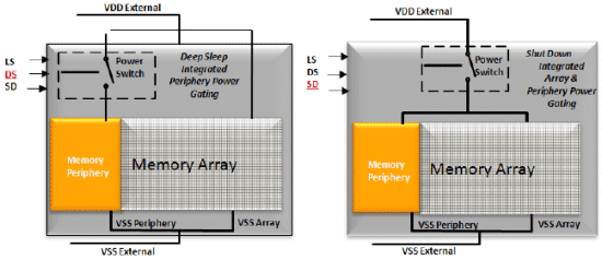
SiWare memory compilers offer advanced power management modes that include Light Sleep, Deep Sleep, and Shut Down. These modes reduce static power through a combination of biasing techniques and integrated power switches and incorporate well with leading embedded processor power management modes.
During Light Sleep, the memory array is biased with retention through a source-diode implementation. Fine-grained power gating is also implemented in peripheral devices. This technique is not sensitive to ground noise because the virtual power nets are short and hidden in the cells. There is also a small wake-up latency and in-rush current at wake-up because the capacitance is limited with this implementation. This mode is enabled with a separate pin.
Deep Sleep and Shut Down modes incorporate internal switches in the memory instance periphery that disable the periphery circuitry or both the memory array and periphery. During Deep Sleep, the switch disables the power supply to the periphery circuitry while maintaining power to the memory array. The memory array is source-biased with the same implementation as Light Sleep mode. The memory array content is retained. In Shut Down mode, the switches disable the power supplied to both the memory array and periphery. The memory array content is not retained in this mode.

Figure 2 - Virage Logic SiWare Integrated Power Gating
The advantages of applying these power management modes are significant. Light Sleep offers up to 50% reduction in standby power with a fast wake-up time. Deep Sleep incorporates a switch that shuts down the memory periphery and source-biases the array with retention. This mode offers a standby power savings up to 70% while Shut Down disables power to both the array and periphery. This mode does not retain the memory array state and saves up to 90% standby power. All of the modes manage the outputs. In Light Sleep the outputs retain the last state. In Deep Sleep and Shut Down modes, the outputs are held low.

Figure 3 – SiWare Memory Compiler Normalized Standby Power Savings
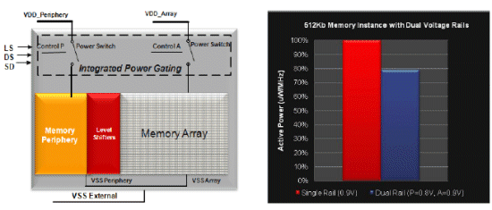
In SoC designs, the use of multiple power supplies is increasing. Voltage reduction for memories is limited by the bit cell. Foundry-supplied bit cells have a minimum voltage specification for retention. This minimum voltage, VDDMIN, may be limited to the nominal voltage, VDDNOM, less ten to twenty percent. Many SoC’s designed for battery-powered applications would greatly benefit from reducing thevoltage to minimize dynamic power. By separating the array and periphery supplies in a memory, designers may meet the bit cell specification for retention within the array while further lowering the voltage in the peripheral circuitry of the memory instance. With memories most likely in the critical path for timing, having the level shifters, clamps, and the memory integrated and characterized as one unit greatly assists in meeting timing closure. The SiWare memory compilers include built-in level shifters in conjunction with power switches.

Figure 4 – Dual Voltage Rail Implementation in SiWare Memory Compilers and Dynamic Power saving example for 40nm G
Optimizing Redundant Memory Reads and Writes
Modern SoC designs have complex data pipelines that perform various specialized computations and interact with processor cores running software. Memories are used to store the results of intermediate computations in the data pipelines, serve as buffers between interacting computations or serve as caches to store frequently read data. Even though locally the reads and writes to a memory may appear to be necessary, it may be the case that depending on the functional mode or complex control sequence of the design, they may not be needed. Removing such redundant memory accesses can result in significant reduction in the dynamic power consumption on memories.
Consider the portion of RTL shown in Figure 5. The design processes two audio streams and switches between the two streams based on an audio_mode_sel control signal. This control could be generated based on the priority of one audio stream or based on some complex algorithm that determines when to process in audio stream based on the rate of incoming samples from that audio stream and the quality of service required for that audio stream. Note that the output of the audio_mem_2 is used only when the audio_mode_sel signal is high. However, both the memories are always enabled by the designer to simplify the read/write control. As a result, both the memories are read or written every cycle, even though the output data from a memory is only used when its audio stream is selected.
In this case, sequential analysis can determine that if audio_mode_sel signal is low and audio_mem_2 is being read, then that read is redundant. Similarly, if audio_mode_sel signal is high and audio_mem_1 is being read, then that read is redundant. Modifying the RTL using this analysis results in the following RTL with the memory enable signals of the two memories gated off when these memories are not used.

Figure 5: Original design and PowerPro MG generated design with observability-based read gating logic inserted (shown in red).
PowerPro MG can automatically analyze a design for conditions under which the value read out of a memory is not used by the downstream logic. PowerPro MG then adds logic to the memory enable to disable such redundant reads. This transformation is called observability-based read gating. In the example above, the observability-based gating condition propagated across one level of sequential logic. But in more complex designs, such conditions can propagate across multiple levels of sequential logic and generate gating conditions to shut off redundant memory reads, thereby saving dynamic power in the memory.
Many memories in designs are read more often than they are written. One example is a memory of coefficients that are used in a digital filter. In such memories, the same address may be repeatedly read without any intervening writes. In such a scenario, all the reads to the same address of the memory after the first one are redundant and can be gated off. Such a transformation is referred to as stability-based read gating since it relies on the stability of the read address and read enable of the memory to gate off redundant reads.
Some issues that are important to consider when generating new logic to gate the memory enable for a memory are:
- The memory enable signal is often timing critical. As such, adding additional logic on the memory enable can result in timing violations. PowerPro MG optimizes the logic required for observability or stability based gating to ensure minimal timing impact.
- If the overhead of creating the memory gating logic is large, then the power saved by shutting off memory operations may be offset by an increase in power due to the gating logic itself. This is also addressed by PowerPro MG. The tool optimizes the gating logic to reduce the power cost of the memory gating logic without impacting its ability to shut off redundant memory operations.
- Flops in the new gating logic need to be reset appropriately when the design powers up to avoid any interference with the reset sequence of the design. PowerPro MG automatically inserts the reset logic to preserve design behavior during reset.
Using Memory Sleep Modes
Memories are often accessed in bursts, resulting in many memory accesses during some time periods, interspersed with periods when memory accesses are not required for the operation of the device. In addition, many design blocks have specialized low activity modes where most of the logic is not active. During such idle periods, the dominant component of power dissipation in the design is leakage power. As discussed above, memory vendors are providing several sleep modes in their embedded memory IP to allow designers to put memories to sleep during idle periods. Such sleep modes are implemented by shutting off the power to various portions of the memory.
In order to use sleep modes effectively, the following key issues need to be taken into consideration:
-
To ensure the functional correctness of a design, the memories must only be put into sleep when no memory accesses are occurring. Further, depending on the timing spec, the memory needs to exit sleep mode some number of cycles before a memory operation can be performed. The number of cycles needed to exit sleep mode depends on how much of the memory is shut off during that particular mode. The deeper the sleep mode, the longer it takes to exit. This requires that the sleep mode control logic must be able to predict when a memory access will occur – a sequential property of the design.
-
There is a dynamic power penalty associated with switching a memory in and out of sleep mode. As a result, if a memory is put into sleep mode, it should stay in sleep mode for a certain minimum number of cycles to actually save power. Figure 5 shows how the minimum number of cycles needed to yield a power saving changes with the operating frequency of the memory and the probability of memory enable being high (memory is active). It is also a function of whether the memory is optimized for fast accesses. Faster memories tend to have a higher ratio of leakage to dynamic power.
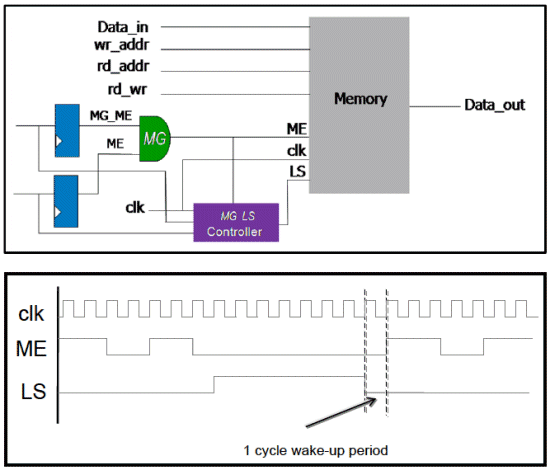
Some memory power saving modes such as shut-down and deep-sleep modes require longer wake-up periods and the designer needs to determine whether to retain the state of the memory or not. As a result, shut-down and deep-sleep modes can be most effectively controlled using architectural states of the design such as block-level idle or sleep states. Light sleep can be performed at a finer level of granularity. PowerPro MG automates light sleep optimization to reduce memory power. Typically, for Virage memories, a single cycle of wake-up suffices which means that the controller for light sleep needs to predict memory operations one cycle before they occur to ensure that the memory is out of light sleep mode in time for the memory access to occur. In addition, the light sleep mode controller added by PowerPro MG ensures that the memory is in light sleep for a sufficiently long duration to save power.

Figure 6: Minimum number of light sleep cycles as a function of memory activity and frequency of operation
PowerPro MG creates additional opportunities for triggering light sleep by performing the read gating transforms, which increase the frequency and duration for when the memory is inactive. Figure 7 shows how PowerPro MG creates a new controller for managing light sleep mode for a memory along with the waveforms of the relevant signals generated by the controller.

Figure 7: Insertion of memory gating to control ME and light sleep mode by PowerPro MG and relationship between LS and ME signals showing 1cycle of wake-up needed for light sleep wake-up. Note that between clock cycles 3 and 5, the PowerPro MG controller does not put the memory into light sleep even though the Memory Enable (ME) is low. However, the memory is in light sleep mode between clock cycles X and Y because it will result in power savings. Also, by exiting light sleep mode by clock cycle Y, the memory can be accessed when ME goes high at clock cycle Y+1.
Design Flow Using PowerPro MG
PowerPro MG fits seamlessly into the RTL design and synthesis flow used by SoC design groups. In addition, PowerPro CG can be used in conjunction with PowerPro MG to insert sequential clock gating conditions in the non-memory portions of the design. In fact, a customer with both PowerPro MG and PowerPro CG licenses can invoke both CG and MG optimizations in the same PowerPro shell.

Figure 8: Flow using PowerPro MG and PowerPro CG as pre-processor to synthesis.
Since the transformations performed by both PowerPro MG and PowerPro CG are sequential in nature, standard combinational equivalence checkers cannot be used to formally verify that the optimized RTL generated by PowerPro MG/CG is functionally equivalent to the original RTL. SLEC Pro from Calypto is a sequential logic equivalence checker that can verify equivalence between designs that have sequential differences internally and at their interfaces. PowerPro MG and PowerPro CG automatically generate scripts needed to run SLEC.
PowerPro MG and CG also provide several other features that facilitate the integration into downstream synthesis/physical implementation flows. Some of these are:
-
ECO flow: in the event of an ECO, PowerPro MG and CG can be run in an ECO-mode, in which the tool determines which of the gating logic inserted by PowerPro on the original RTL is still functionally valid and generates an ECO file indicating which gating logic needs to be disabled.
-
PowerPro Analyzer for visualization of the gating logic inserted by PowerPro CG or MG.
Case Study
A design block from a networking chip will be used to illustrate the power savings achievable using PowerPro MG. The block has 14 embedded memories that account for about 40% of the total block area and 50% of the total block power. Further, the distribution of total memory power between dynamic and leakage power is 60% and 40%. The numbers were computed using a third party synthesis and power estimation tool post synthesis and are based on a representative switching activity file for this block provided by the customer.
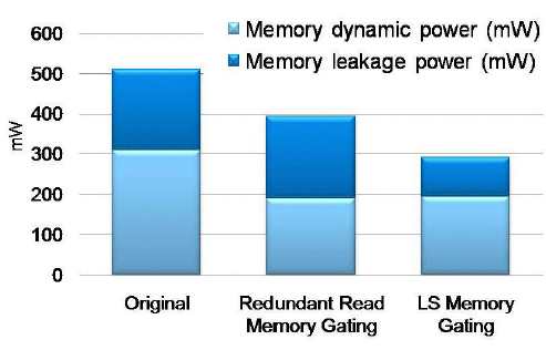
When this design was run through PowerPro CG and PowerPro MG, PowerPro CG was able to reduce the dynamic power in the non-memory portion of the design by 15%. PowerPro MG found observability-based read gating moves on 5 of the 14 memories which reduced the number of reads on these memories from 50% of the clock cycles to only 3% of the clock cycles. The result was a 40% reduction in dynamic memory power. Light sleep memory gating was then used. Light sleep control logic was inserted for all the memories, resulting in 55% reduction in the memory leakage power. As a result, overall memory power was reduced by about 45% and the total design power was reduced by approximately 30%. Figure9 shows the change in dynamic and leakage power of the memories in the design as a result of removal of redundant reads, followed by insertion of light sleep controllers.

Figure 9: Change in memory power components as successive optimizations are done in PowerPro MG.
Conclusions
Removing redundant memory accesses and utilizing the low power modes in embedded memories requires sequential analysis of the design across multiple pipeline stages. Many RTL designs have significant room for memory power reductions due to non-local observability or stability conditions that are very hard for designers to account for manually as well as time consuming to verify them. PowerPro MG automates the sequential analysis, power/timing/area tradeoffs and generation of optimized RTL for memory optimizations. SLEC provides comprehensive formal verification of the optimized design. PowerPro CG and PowerPro MG provide a complete set of automated transformations to reduce power in all portions of a design.
References
Ramachandran, Venky. “Minimizing Power Consumption in RTL Designs Using Sequential Clock Gating and Low-Power Synthesis.†EDA Design Line. 26 May 2009.
