By Gerard Boudon, IBM Microelectronics
Abstract:
Because the dimensions of lithography are now closer to the fundamental physical limits, scaling is more and more difficult and thus multi-core processor solutions are just starting to be more popular in the embedded area. This paper describes in details the features that allow SoCs to be built with up to eight 1.6 GHz PowerPC CPU cores in an embedded system supporting Symmetric Multiprocessing (SMP) architecture. The balancing between CPU execution speed, memory bandwidth and latency, and coherency overhead has been the objective of the design of the PLB6 and the L2 Cache IP's, to reduce as much as possible the drop-off in performance-per-core inherent in an SMP approach.
1. Introduction
In September 2009, [1] IBM has introduced an 1.6 GHz PowerPC CPU IP in 45nm SOI - 3.6mm2 size - that can be integrated in multi-core system-on-chip (SoC) product families for communication, storage, consumer, and aerospace and defense embedded applications.
2. PowerPC476 IP
The PowerPC 476FP embedded processor core is a 5- issue, 5-pipeline, superscalar, 32-bit reduced instruction set computer (RISC) processor. The core supports the Power Instruction Set Architecture V2.05. The core also supports memory coherency to broaden ASIC solutions into multiprocessing system environments and to increase its scalability.
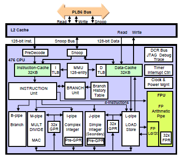
The overall organization of the processor core is shown on Figure 1 .
Instruction Path
The PowerPC 476FP processor is a high performance core with capability to issue up to 5-instructions per cycle. These instructions can feed in parallel the following five fixed point units as well as the separate floating-point (FP) pipeline:
- Branch pipeline
- Load and Store operations
- Simple arithmetic and logical operations
- Simple and complex instruction pipeline,
- Multiplication and division pipeline
L1 Cache
The L1 32 KB Instruction and L1 32 KB Data caches are two-cycle pipelined cache accesses, with index of real address in the 1024-entry unified translation lookaside buffer (UTLB)
The L1 Cache Address and Data Caches are snoopable. Early delivery of instructions to the floating-point unit is enabled because all instructions are predecoded
Floating-Point Unit
The floating-point unit (FPU) is a pipelined, doubleprecision math computation processing unit that is attached to the processor core. The FPU conforms to the IEEE Standard for Binary Floating-Point Arithmetic. The FPU is a Six-stage super-pipelined floating-point arithmetic execution with independent floating-point load-and-store and execution units

Figure 1: PowerPC476 CPU core block diagram
Power Saving
The PPC476FP includes design features to minimize the operating power of the PowerPC 476FP
- All latches are clock gated so that idle functions do not waste power.
- All non executing and idle functions are disabled.
- Static random access memory (SRAM) is partitioned so that only the required memory zone is enabled or selected.
- Doze and idle sleep modes are available.
- The central logic and the floating-point unit have separate clock enables
3. L2 Cache
The L2 Cache IP [2] can be configured in 256K, 512KB or 1 MB with a maximum of 4,096 entries. The L2 cache line is 128 byte and the cache is 4 way set associative. To support the high RAS (Reliability and Serviceability) requirement of the networking application, the L2 Cache arrays are protected by Parity and ECC bits.
| IP | Size (bits) | Protection |
| L2 Cache | 4,096x128x8x4 | ECC |
| Cache Tag | 4,096x36x4 | ECC |
| LRU | 4,096x30 | Parity |
Table 2 : SRAM array inside a 1MB L2 Cache IP.

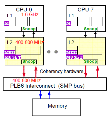
Figure 2: SMP implementation with the PPC476 showing L2 Cache states
4. PLB6
The 476FP “subsystem†which includes the PowerPC 476FP CPU core, the Level 2 cache/cache controller, is connected to other “subsystems†through the PLB6, the latest architectural extension of the CoreConnect local bus architecture. This structure enables SoC designers to easily and rapidly develop entire families of products, scaling the number of “master†cores from 1 to 16 (including 1 to 8 Coherent CPU cores) on the bus. The PLB4 CoreConnect internal Bus is a shared bus of 128bit data at a maximum speed one fourth of the CPU speed. It was designed for sub 1GHz CPU cores. High performance is achieved with a dual bus structure one bus with a high throughput and the second with low latency. Each of them is independently capable of handling read and write operations at the same time.
The new IBM CoreConnect PLB6 bus looks more like a fabric with high speed point to point links, with each of them having 128 bit Read and 128 bit Write Data paths at one half of the CPU clock speed.
The bus fabric on the PLB6 is capable of supporting up to 8 coherent master elements, giving SoC designers the flexibility to mix and match I/O masters, processors and other accelerators within the fabric.
The high throughput of this bus is due to its fabric structure with up to eight slave segments, that can simultaneously receive or transmit Data.
Each slave segment may have up to 4 slaves. It is possible, in 45nm technology and without any preplacement in silicon, to operate the bus structure at up to 800MHz.

Figure 3: Master and Slave attachments to the PLB6 CoreConnect bus
Symmetric Multiprocessing (SMP)
In order to guaranty coherency between data in main memory and data in the various caches, the design of a conventional SMP system is following the MESI protocol:
- M Modified
- E Exclusive
- S Shared
- I Invalid
These states are associated with each cache line (L2 for the PPC476). Each CPU performs snooping operation where these cache states are used. Notice that the cache in the SMP processors architecture must have the same Cache line size and the same MESI states.
The performance of such coherent SMP system is limited by the fact that transactions are possible only between the Cache and the main memory. For example, when a CPU 1 wants to read a data that is in a M (Modified)
state in the cache of a CPU2, the first operation is for the CPU2 to write the Data in the memory, and then the CPU1 can read it. Result; 2 operations with 2 memory access are needed for CPU1 to get the data.
With the symmetric multiprocessing architecture, scaling up the number of processors, is efficient if at the same time the hardware coherency is smart enough to handle the huge bandwidth demand of the coherence transactions.
It is necessary to have a non-blocking coherence resolution which prevents stopping CPU execution most of the time; In the PPC476 three additional states are introduced in the L2 cache in order to allow Cache to Cache transfer, and better Atomic operations.
The Data transfer is eased by a dedicated path between different subunit called Intervention data path. These 3 states are:
- MU Modified Unsolicited
- T Tagged
- SL Shared Last
Intervention
The purpose of intervention by a CPU Master is to reduce the latency needed to fetch a cache line when it is not present in its L2, but is present in other L2’s.
The SL (Share Last) state is used for Intervention. It designate one (only) cache responsible to provide the Data after an intervention. As result of an intervention among L2’s, Cache to Cache transfer is done instead of Memory access after a L2 miss.
5. Example of SoC implementation
An example of system implementation is shown in figure 4. The PLB6 is mainly reserved for high speed access and for handling memory coherency due to the use of multiple CPU cores. The System Memory is also attached to the PLB6 because fast access to memory is very important for running code and provides data not already in cache. Due to high speed of the CPU it is necessary to provide data from main memory at a speed that only the late generation of DDR3-1600MHz SDRAM can give.
A SoC requires also high speed I/O’s, that are attached here below a PLB6 to PLB4 interface. These I/O are commonly PCI Express with second generation 5gbps per port throughput. Legacy Ethernet is also mandatory because it is important at least to load code in the system. Other IP blocks such as USB or SATA can be connected through an AXI bus for example.

Figure 4. Example of SoC based on the PPC476 IP
6. Physical implementation
SOI: In order to reduce power and electrical leakage, the choice of 45nm silicon-on-insulator (SOI) technology was made. SOI can provide up to a 30 % chip performance improvement and 40 % power reduction, compared to standard bulk silicon technology [3]. This technology is used by IBM in a wide range of application-specific integrated circuits (ASIC) and foundry clients as well as in chips for its servers and storage products.
For performance and power dissipation optimization, the PowerPC476FP CPU IP has been designed in a hard core, while for flexibility in personalization, L2 cache and PLB6 are synthesizable; see layout of the PPC476 core on figure 5. The following table indicates various areas of the IP block necessary to build an SMP system.
| IP | Size | |
| PPC476 | Hard Core IP | 3.6 mm2 |
| L2 Cache | Soft IP | 4mm2 * |
| PLB6 cntl | Soft IP | 0.035mm2 ** |
* 512 KB L2
** Masters 4 C + 1 - Slaves 1C + 2 (C=Coherent)
Table 2: Core size in 45nm SOI technology.

Figure 5: PowerPC 476 CPU 3.6 mm2 hard core
7. Design verification by emulation
Functional verification of the PowerPC 476FP CPU, L2 cache and PLB6 bus complex made extensive use of hardware emulation through a custom multi-core FPGA based test board. In addition to greatly speeding up the design verification effort, this emulation platform has provided for Linux kernel and device driver configuration and testing, and it is providing for extensive early code development and benchmarking.
8. Conclusions
It has been agreed in the industry that the future of embedded system is multi core. The PPC476 includes 3 key IP cores; the 1.6GHz CPU, the L2 cache and the PLB6, which combined together, helps SoC designers to built embedded system with the highest performance. This performance is achieved with the coherence of data managed by hardware assist.
9. Acknowledgements
Thanks to the IBM PowerPC design team for providing information used to prepare this paper.
References:
[1] B. Talik “Introduction to the New High-Performance IBM PowerPC 476FP Core†- Linley Tech Processor Conf Sept 17,09.
[2] W. Nation “Multicore Processor Cache and Subsystem Design for a High-Performance PowerPC Targeting Networking and Storage†- Linley Tech Processor Conf Sept 17,09.
[3] R.Pottier & al "ARM 1176 implementation in SOI 45nm technology and silicon measurement" IEEE International SoI Conference Oct 2009
