João Vitor Bernardo Pimentel a, b
José Camargo da Costaa
a Universidade de BrasÃlia – BrasÃlia, Brazil
b Czech Technical University in Prague – Prague 6, Czech Republic
Abstract:
The development of analog IP blocks shows its own difficulties in that it is still unclear, today, what characteristics those blocks must actually have and how they should be approached. Particularly, there is no broad, openly available stardard for analog IP.
This work attempts to help solve this lack of standardisation by presenting a methodology for describing analog integrated circuits (or analog portions of more complex designs) as intellectual property blocks. The main aspects of analog IPs are reviewed, along with brief guidelines on how to deal with them. The proposed methodology is exemplified and evaluated through its application to two different analog/mixed-signal integrated circuit blocks, which showed good results.
1. INTRODUCTION
The use of IP blocks shows great advantages to both providers and users. However, the use of analog IP is still much less significant than that of digital IP [1]. That is partly because analog circuits, usually having stronger restrictions, tend to be less reused [2]. Another matter is the lack of consensus, today, on what should be required from an analog IP.
In this work, developed at Universidade de BrasÃlia, we present a methodology for achieving an analog hard IP from a starting or previous design. The main desired characteristics of an analog/mixed-signal (AMS) IP were reviewed and previous efforts in standardisation were studied in order to achieve a methodology that is broad and widely available. That is why it was planned to be somewhat compatible with the two stronger standards for analog IPs, the Virtual Socket Interface standard [3] and Freescale's Semiconductor Reuse Standard [4]. In spite of their importance, the first is already eight years old and will not be revised any longer, and the SRS is only partially available for developers outside Freescale. Therefore, a new, broader approach would be quite useful.
The proposed methodology is detailed in the next section. In Section 3, its application in two AMS blocks is described, to exemplify the methodology and to study and evaluate its main advantages and flaws. Some results obtained in the cases studied are presented in Section 4. Section 5 concludes the work presented.
2. METHODOLOGY
The methodology proposed here intends to help analog circuit providers to complement their design flows in order to achieve an IP block from a standard analog design, as well as facilitating the reuse of the block. It can be applied from the start of the project or after a version of the design has been completed. Of course, if the creation of a virtual component (VC) for reuse is considered in the initial stages of the design, many factors (e.g., testability) can be taken into account early on. This may shorten the time needed for future adaptations and reduce possible differences between the original and the adapted blocks.
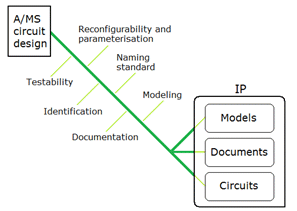
Figure 1
The basic idea, shown in Figure 1, is to provide guidelines for analog circuit designers so that a given analog circuit block can be traded as IP. This can be done if certain steps are taken during the design:
- ensuring it shows characteristics that are compatible with the concept of IP;
- elaborating high abstraction level models of the circuits;
- developing the adequate documentation.
The features a circuit block must present to correspond to what is expected of an analog IP, as can be found in related bibliography, are listed in Table 1 and discussed briefly in items 2.1 to 2.6.
| Characteristic | Goal |
| Reconfigurability/parameterisation | Reuse in different applications |
| Testability | Allowing validation by the user |
| Naming standards | Easier integration and simulation |
| Identification | IP protection and easier integration |
| Modeling | IP protection and validation by the user |
| Documentation | Allowing a correct use of the VC |
Table 1
2.1 Reconfigurability and parameterisation
The possibility of reconfiguring a circuit for different specifications improves its potential for reuse in different systems [2] and therefore is desirable in IPs. This can be done by including reconfigurable structures in the design (likely creating obstacles for optimization) or, alternatively, parameterising some aspects of the design. Parameterisation makes it possible to create a library of cells, all based on the same design but with different specifications (which can mean greater optimization, but also an increase in the the time required to achieve the final designs [5]). These concepts are illustrated in Figure 2.
2.2 Testability
If a given circuit is going to be reused as an IP, it is important that integrators (who may not know its internal topology) are capable of verifying some of its characteristics, in order to validate their own systems. Thus, the providers of the IP should ensure some observability and controllability to it, through what is called design for testability (DfT): including in the design test structures or defining test procedures which cover the whole expected range of operation for the circuit. There are DfT techniques applicable to analog circuits (such as in [6]); in any case, test structures should impact circuit performance as little as possible.
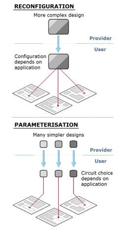
Figure 2
2.3 Naming standards
Pins and signals should be named in a way that is unambiguous, comprehensible and useful. It is recommended that names begin with a prefix indicating the block to which they refer, followed by an indication of pin or signal type (analog or digital, voltage or current, operation mode, and so on), and finally an indication of its function in the block [7]. Also, names should preferably be all written in lowercase.
2.4 Identification
Tags should be used to help track the use of virtual components in a design. This can be done as comments in HDL codes or as text in an adequate layer of a layout. Some information should always be included in an IP tag: the name of the vendor, the product (i.e., the circuit block) and its version. In this work, the pattern proposed for the tag is derived from the VSI standard, with one format for tags within models and another for tags in layout files, as shown in Table 2.
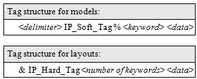
Table 2
The delimiter, in Table 2, is whatever sequence of characters that is used to separate codes from additional information (commentaries) in the language in which the models are written. For layouts, the delimiter is always the character '&'. In both cases, the keyword identifies what the following data refers to. The sets “% <keyword> <data>†or “% <keyword> <data>†can be inserted as many times as desired, to insert additional optional information.
The field number of keywords is included for layouts because GDSII files have limitations to the number of characters in a text line that HDL codes usually don't, so tags may take more than one line. Also, it is useful to know how many optional keywords there are, and to identify them; it is proposed that optional keywords begin with the underscore character ('_'). These aspects of the tags make them easier to understand or to automatically scan the IP for tags.
2.5 Modeling
For complex systems, high abstraction level models are useful in that they allow different functionalities to be analysed with relative ease. In the context of IPs, a black-box model is also an invaluable tool for potential users: it allows them to decide whether to use a certain block in different systems (or in different configurations) with much more clarity than by just analysing the block's specifications [8].
There is a trade-off between the complexity of the model and how much lighter it is in computational effort than an electrical simulation, so it is useful to have models in different hierarchical levels. For this work, several references dealing with AMS IPs (such as [1], [8] - [10]) have been studied to reach the proposed division, shown in Table 3. It is recommended that the models are written in a description language that is easily accessible by potential users, preferrably with equivalent models in different languages.
2.6 Documentation
The documentation for the IP should include every information that the user needs to make full use of the virtual component: a full description of the modes of operations, how to test, how to integrate, known problems, and so on. There is a trade-off between the level of details shown and intellectual property protection, but it is possible to describe all an integrator needs to know without revealing the circuit's topology or other sensible information. The provider has the choice of depicting or not the internal architecture of the block.
| Level | Description |
| Functional | Block's ideal behaviour; no depiction of internal structure or sub-blocks |
| Behavioural | Incorporates non-ideal behaviour to the model, while keeping the structure hidden |
| Structural | Describes the circuit by describing the behaviour of a set of sub-blocks and their interconnections |
Table 3
The information should be relevant and divided in an organized way, in different documents with well-defined and non-redundant contents. The proposed set of documents is shown in Table 4, along with a brief description of the contents of each document.
| Document | Contents |
| Basic Information | Short, 1-page document with essential information (vendor, product and version, main specifications, etc.) |
| User Guide | Detailed description of functionality and specifications (operating ranges, modes of operation, known problems, etc.) |
| Creation Guide | Information about the creation of the block (version history, principles of operation, design methodology, etc.) |
| Test Guide | Procedures for testing and validating the block and related information (conditions, signals, expected results, etc.) |
| Physical Implementation | Information on the physical implementation of the IP (floorplanning, pin requirements, manufacturing technology, etc.) |
| Models | High-level model codes and detailed description (requirements for simulation, description of parameterisation, testbenches, etc.) |
Table 4
3. CASE STUDIES
Two previously designed circuit blocks were used as case studies for evaluating the methodology proposed here: a voltage-to-current converter (which will be abbreviated to VI) and an analog-to-digital converter (ADC). Both circuits are part of a SoC (System on Chip). The VI was designed after the ADC, to act as interface between the ADC and external sensors and their signal conditioning circuitry. These blocks were designed for a given purpose, and adapted for use as IP through the procedures described in this work.
The VI, for instance, went through all the steps of the presented methodology. Although it would require a lot of space to detail all the modifications made to the circuit, in Figure 3(a) is shown the original structure of the circuit, while the adapted structure is shown in Figure 3(b). These modifications allowed reasonable degrees of reconfigurability and testability by inserting switches and additional outputs to the circuit, which result in three additional modes of operation to the circuit, and allow testing the functionality of each sub-block. This was achieved without increasing the area needed for the circuit, since the new structures were placed in “empty spaces†in the original design.
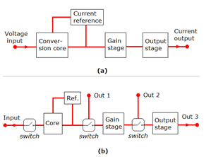
Figure 3
The naming standard and indentification were enforced during the adaptations to the circuit. After validation of the new structure of the block, VHDL-AMS models were created from the ideal specifications and from the simulated electrical behaviour of the circuit. Finally, a set of documents was elaborated, according to the division in Table 4. This documentation is different from documents intended for internal use, as they do not reveal internal topology or sizing.
The ADC did not require many adaptations to the block, because the original circuit already included test structures and some reconfigurability. Therefore, it was made adequate to what is proposed in this work by including identification tags, standardising pin and signal names, and by creating high-level models (in VHDL-AMS) of the block, as well as generating extensive documentation, according to what is described in Section 2.
4. RESULTS
The VI's performance was kept within specifications without any increase in die area, by using the available space between sub-blocks to place the small test structures. At the same time, power consumption has been reduced. VHDL-AMS models of the VI were developed from information available from electrical schematics and simulations, so that the final result were models that are coherent with the behaviour of the original circuit and that can be simulated by users without any knowledge of the real circuit. Figure 4 shows the output characteristic of the VI for several temperatures in (a) the original circuit, (b) the adapted circuit and (c) the behavioural model.
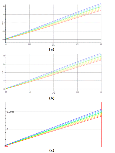
Figure 4
For the use as IP, an adequate documentation, following the guidelines proposed in section 2, was generated. It is detailed enough to allow integration and use in systems apart from the SoC to which it was originally intended, and yet no description of the internal topology is needed. The ADC went through similar procedures. In the end, both circuits are adequate to be traded as IPs.
5. CONCLUSION
This work briefly presented a methodology proposition for adapting analog and mixed-signal integrated circuit designs to what is expected of IP blocks. Applying this methodology to previously designed blocks achieved good results, consistent with the goals of the proposal: both IP blocks present the desired characteristics and can be fully used by third parties without knowledge of their internal topologies. This was achieved by means of modifications in the design, high-level models and an adequately elaborated documentation.
For the future, further studies can allow this methodology to be applied to firm IPs (parameterised descripitions of circuits which the user optimizes). Other analyses (e.g., with more critical designs, or comparisons between blocks from different providers) may allow further improvements on the methodology.
6. REFERENCES
[1] Gielen, G.G.E. and Rutenbar, R.A., Computer-Aided Design of Analog and Mixed-Signal Integrated Circuits, Proceedings of the IEEE, vol. 88, nº12, 2000.
[2] Saleh, R., Wilton, S., Mirabbasi, S., Hu, A., Greenstreet, M., Lemieux, G., Pande, P.P., Grecu, C. and Ivanov, A., System-on-Chip: Reuse and Integration, Proc. IEEE, vol. 94, nº 6, USA, 2006.
[3] VSI Alliance, Analog/Mixed-Signal VSI Extension Specification (version 2.2), 2001.
[4] Freescale Semiconductor, Semiconductor Reuse Standard – Documentation (v 3.2), 2005.
[5] Li, Z., Luo, L. and Yuan, J., A Study on Analog IP Blocks for Mixed-Signal SoC, Proceedings ASIC, pp.564-567, Beijing, 2003.
[6] Looby, C.A. and Lynden, C., Field Programmable Analogue Arrays: a DFT View. IEE Colloquium on Testing Mixed Signal Circuits and Systems, 1997.
[7] Pimentel, J. V. B., Metodologia para Descrição de Células Analógicas como IP, M.Sc. Dissertation, Universidade de BrasÃlia, BrasÃlia, 2009.
[8] Vandenbussche, J., Gielen, G. and Steyaert, M., Systematic Design of Analog IP Blocks, Kluwer Academic Publishers, Netherlands, 2003.
[9] Levi, T., Tomas, J., Lewis, N. and Fouillat, P., IP-Based design reuse for analog systems, Proc. SPIE, vol. 6590, France, 2007.
[10] Hamour, M., Saleh, R., Mirabbasi, S. and Ivanov, A., Analog IP Design Flow for SoC Applications, University of British Columbia, Canada, 2003.
[11] Castro-López, R., Fernández, F. V., and Vázquez, A. R., A reuse-based framework for the design of analog and mixed-signal ICs, Proceedings of the SPIE, 5837(3), pp. 25-36, 2005.
7. ACKNOWLEDGEMENTS
The authors would like to thank CNPq and Instituto do Milênio – NAMITEC (Brazilian governmental agencies) for financial support.
