By Nanjundaswamy H R (NeST Software private Ltd), Divya B S (Acharya Institute of Technology, India)
Bangalore, India
Abstract:
This paper is presented with the Video Graphics Array (VGA) and Digital Visual Interface - Digital (DVI-D) test pattern generator solution with display monitor timing specification as per the Video Electronics Standards Association (VESA) to address the VGA and DVI-D video processors RTL verification and chip validation requirements.
Synthesizable VESA-VGA and DVI-D test pattern generator core developed using Verilog Hardware Description Language (HDL) could be used for the chip verification and the same core implemented onto Field Programmable Gate Array (FPGA) to function as VESA-VGA and DVI-D test pattern signal source for chip validation.
1. INTRODUCTION
VGA and DVI interface has been the one of the interfaces for the computer monitor and projector units.
VGA (Video Graphics Array) is a basic standard for color resolution in computer monitors. Video Electronics Standards Association (VESA) had released a similar standard referred to as Super VGA (SVGA). XGA was capable of 65,536 colors at a resolution of 800 x 600, or 256 colors at 1024 x 768, similar to early SVGA standards. Accordingly, Super XGA (SXGA), Ultra XGA (UXGA) and Quad XGA (QXGA) followed, along with many others.
DVI is the accepted standard for transferring serially uncompressed digital data at high speeds between a Personal Computer (PC) host and a digital display, such as an Liquid Crystal Display (LCD) monitor. DVI-D enables a video signal to be transferred from a PC source to a digital display in its native digital form, simplifying the way PCs communicate with displays and improving display image quality. DVI can be used to deliver single or dual-link digital video to a display device.
VGA and DVI-D video processors Register Transfer Level (RTL) verification requires the input test pattern HDL core for the simulation and validation of processor chip require the hardware test pattern signal source.
This paper aims to address the solution for such requirements.
2. VESA – VGA and DVI – D TEST PATTERN GENERATOR VERILOG – HDL ARCHITECTURE

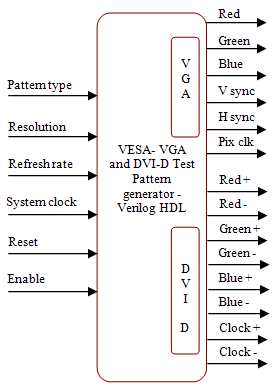
Fig . 1. VESA – VGA and DVI – D Verilog – HDL core interface signals
Synthesizable VESA – VGA and DVI–D test pattern generator core developed using the Verilog – HDL with display monitor timing specification as per the Video Electronics Standards Association (VESA). The top level interface signals of the core shown in Fig.1.
The core is programmable to:
- Video pattern type
- Resolution
- Refresh rate
The output video test pattern with pixel size of 8 bit Red, Green and Blue with Vertical Sync (V Sync), Horizontal Sync (H sync) and pixel clock (Pix clk). The enable signal is provided to enable (logic ‘1’) or disable (logic ‘0’) the pattern generator core. Pixel clock is the internal requirement for generating the test pattern stream and Pixel clock made available on port.
For the RTL simulation requirement the test pattern generator internally generates the respective pixel clock based on the display monitor timing specification and this pixel clock generator module is not synthesizable.
The FPGA implementation of test pattern generator core makes use of 100 MHz board clock and FPGA vendor specific clock generator logic modules to generate the respective pixel clock.
The VESA – VGA and DVI–D test pattern generator core HDL code is default for RTL simulation and +define FPGA compiler directive to port onto FPGA.
3.1 Video pattern type supported
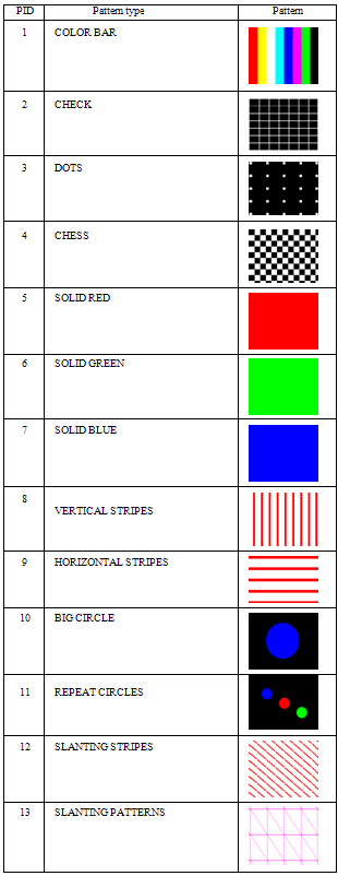
There are thirteen types of video patterns are supported listed in the TABLE 1.
As such deriving number of video patterns is the not the limitation with the available pattern types varying the color combinations many video patterns could be realizable.
Since a configurable design, could be possible to implement new video pattern types. The default resolutions type is COLOR BAR.
TABLE. 1. VIDEO PATTERN TYPES

3.2 Resolution supported:
There are number of resolutions de-facto standards have been used with computer display monitor. These are usually originated by video display adapter manufacturers. VESA group has coordinated with several leading video display adapter manufacturers.
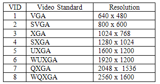
VESA – VGA simulation mode supports eight types of video standard types with display timing information described by VESA are listed in TABLE 2. The minimum 640 x 480 (VGA) @ 60 Hz with pixel clock 25.175 MHz and the maximum of WQXGA(Widescreen Quad Extended Graphics Array) with 2560 x 1600 @ 60Hz with pixel clock 268 MHz
DVI- D simulation mode supports single link DVI. The lowest pixel clock required by DVI is 25.175 MHz which equates VESA – VGA 640 x 480 @ 60 Hz. A single DVI link has a bandwidth of 165 MHz, which equates to 165 million pixels per second. The maximum data rate supported for the single link DVI is 3.96 Gbit/s (165 MHz x 24 bits). VESA – UXGA with display monitor timing specification of 1600 x 1200 @ 60 Hz with 162 MHz matches to support under the maximum single link DVI data rate is supported in the pattern generator RTL core.
VESA – VGA and DVI–D test pattern generator core on FPGA tested up to XGA (1024x768@60 Hz) 65 MHz pixel clock with 24 bits pixel depth.
TABLE .2. RESOLUTION TYPES

3.3 Refresh rates supported:
There are five type of refresh rates listed in TABLE 3 are supported. VESA describe the specific number refresh rates for the different video standards. Depending on the video standard selection design allows to choose respective supported refresh rate.
TABLE .3. REFRESH RATE TYPES

3. TYPICAL RTL SIMULATION SETUP
In the RTL simulation requirement VESA – VGA and DVI–D test pattern generator core is instantiated into the design verification testbench drives the VGA and DVI-D transmitter interface signals. Fig. 2, shows the typical simulation set up

Fig. 2. Typical simulation setup
4. SIMULATION
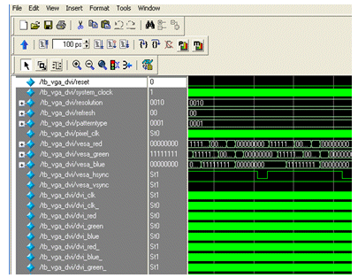
Fig. 3 shows the VGA color chess generation verification wave form. In case of RTL simulation the video data available to dump in a PPM (Portable Pixel Map) file can be viewed by PPM supported image browsers, this option allows to check the test pattern generator functionality.

Fig. 3 HDL simulation waveform
5. TYPICAL CHIP VALIDATION SETUP

Fig. 4. Typical system level testing setup
The synthesizable VESA – VGA and DVI – D test pattern generator Verilog – HDL core ported onto FPGA to drive as VGA and DVI –D test pattern source.
Pattern generator default setup is VESA – SVGA 800 x 600 @ 75 Hz same data would be available on DVI-D port.
There are three toggle keys to set in on-hot way to select configure the Video pattern type (001) listed in Table 1, Resolution (010) listed in Table 2 and Refresh rate (100) listed in Table 3. A push button key used to increment Pattern Identification (PID), Video Identification (VID) and Refresh Identification (RID) based on the toggle keys position.
A character display shows the present ID and the changed ID while configuring. Fig. 4, shows the typical system testing set up.
6. SYSTEM TESTING
Fig. 5 shows the color chess generation setup implemented on FPGA (Field Programmable Gate Array) and the output connected the VGA monitor.
Fig. 6 shows the color bar generation setup implemented on FPGA (Field Programmable Gate Array) and the output connected the DVI-D monitor. TMDS (Transition Minimized Differential Signaling) pins are used on FPGA board to drive (Red, Green, Blue and Clock)

Fig. 5 FPGA implemented VGA pattern generator setup

Fig. 6 FPGA implemented DVI-D pattern generator setup
7. CONCLUSIONS
Video Graphics Array (VGA) and DVI –D (Digital Visual Interface) test pattern generator solution developed as per the Video Electronics Standards Association (VESA) display monitor timing specification was used in the a video processor RTL simulation and chip validation. The design can be upgradable to HDMI (High-Definition Multimedia Interface) pattern generator solution.
8. REFERENCES
1. VESA and Industry Standards and Guidelines for Computer Display Monitor Timing : Version 1.0, Revision 0.7 Revision Date: 12/18/96
2. Digital Visual Interface, Revision 1, 12 April 1999.
About the authors:
Nanjundaswamy H R is Engineering - Project manager at NeST Software private ltd, India in VLSI division. He is a VLSI and embedded systems engineering professional since from 1995, extensively worked for image, audio and video products design. Co authored the image processing book for university undergraduate course. He is an electronics engineering post graduate. His research interests are multimedia, wireless communication and processor design.
Divya B S is a senior lecturer in the department of electronics and communication engineering at Acharya Institute of Technology, Bangalore since 2005. She is an electronics engineering postgraduate. She is been teaching image processing and embedded system design course for the for graduate and postgraduate engineering program under a Technological University in India. Co authored the image processing book for university undergraduate course. Her research interests are in image processing and embedded systems designing.
