Frank Schirrmeister, Achim Nohl, Drew Taussig
Synopsys Inc.
Abstract
In this paper, we will outline a solution for prototyping, programming and implementing Application Specific Instruction-set Processors (ASIPs). A general introduction into this class of processor architectures and their characteristics is provided. An H.264 design example using the LISA language for ASIP design will be introduced. The effects the usage of ASIPs can have on the verification efficiency will be discussed in detail, specifically the ability for designers to separate hardware verfication from functional verification.
Introduction
Electronic product evolution always follows the same path: perform more functions, do them faster, and be at a lower cost. This is coupled with pressure on design teams to reduce time-to-market and lower development costs. As a result, products need to be designed faster, have to be re-reusable for multiple derivatives, and have to scale with growing performance demands.
Increased performance is driven by two factors, computational complexity and data rates. More computational operations have to be performed on more data samples in a constant time window. Evidence for this trend can be found in application domains like video processing, wireless communications, and industrial automation.
For video, high definition (HD) is the de-facto consumer standard. In order to not exceed the channel bandwidth for broadcasting, HD video is encoded with more advanced and computation intensive video codecs such as H.264. In the wireless domain, the symbol rates are increasing dramatically with the new LTE standard. In order to achieve these rates using the same frequency spectrum, more complex algorithms are used for encoding and decoding. For industrial automation, a robot micro-controller has to perform more operations per second to manufacture more products per day.
In all examples frequency scaling is no longer an option. Either the design is already operating at the frequency limit or a higher frequency would violate power constraints As a result, parallelization and specialization of hardware platforms must be employed to achieve the necessary energy efficient performance (MIPS/mW). This specialization implies that designs are fixed, which contradicts with another emerging requirement: flexibility.
Video and wireless subsystems need to handle multiple standards and modes. Even after tape-out they need to be flexible enough to accommodate unforeseen updates and changes.. Specialization also implies risks for the design. A single requirements that has not been captured exactly right during the specification phase may result in an un-usable design. So called Application specific instruction-set processors (ASIPs) have emerged as a solid solution where specialization does not result in loss in flexibility, and this flexibility does not compromise performance and power goals.
Finally, verification has become another reason to re-think design flows. Verification has long dominated the chip development effort, specifically the need to functionally verify the design prior to tape out has reportedly been taking up to 70% of the chip development effort. Part of the challenge for verification is the ability to effectively describe all requirements hardware blocks have to meet and then to run verification checking all requirements. Given the flexibility today’s hardware blocks need to meet – as described above – this challenge has been increasingly difficult to meet for dedicated hardware blocks. ASIPs offer an interesting alternative and improvement to the design flow as they allow the separation of actual hardware verification and functional verification. Once designers have confirmed that an ASIP meets the defined functionality, functional verification of the algorithms to be executed on the ASIP becomes verification of the software running on the ASIP anc can be done in parallel to hardware implementation.
Introduction to ASIPs
The term ASIP is widely used in industry and academia to classify programmable architectures that are tailored to a specific class of applications and algorithms. However, the attribute “application specific†does not necessarily refer to just a software application. Instead, it refers to the application of a processor in a specific system context, performing specific functions with distinct design goals.
An ASIP has to be designed and implemented in a way that ensures the entire system meets its design goals. Often the instruction-set of the processor is considered to be the main attribute that makes a processor application specific. However, with the broader view of an application, two other characteristics become equally important: interfaces and micro-architecture. The interfaces define how the architecture interacts with the system for communication and control.
For data intensive algorithms, communication interfaces can quickly become a bottleneck if they do not map to the way data is consumed and produced by the algorithm and the surrounding system. Just tailoring the instruction-set of a RISC type architecture with highly parallel and specialized instructions is not enough if, for example, the load/store unit of the processor cannot handle data fast enough. The architecture of an interface can be just as important as the bandwidth.
A load/store type of architecture already implies a scheme for how data is consumed and produced which may not reflect the way it is demanded by the algorithm or and surrounding system. Often, data has to be passed through a whole pipeline of functional blocks which are inter-connected via specialized FIFOs. The same holds true for the way data is processed internally in the ASIP. The pipeline of an ASIP needs to be designed in a way that matches the way data has to be processed to achieve the frequency goals.
A traditional RISC fetch, decode, memory, execute, write-back scheme can become counterproductive for the design. ASIPs, e.g. for Turbo Decoding in LTE [1] can easily have 15 stages, each one of them containing dedicated processing units using internal and external interfaces.
In terms of the instruction format, ASIP instructions often do not match the classical format which is composed of a mnemonic and register/memory operands. Instruction operands define the internal communication between functional units, and the external communication using the ASIP interfaces. The number, format and type of instructions of an ASIP follow the flexibility requirements of the design. In general, instructions activate certain functional units in the design along with the configuration of register/memory address lines. A classical processor uses general purpose registers for inter-unit data flow. In case of a hardware design, the dataflow is mostly hardwired or controlled via configuration registers. An ASIP can implement both equally efficiently. For mostly constant operands, implicitly used configuration register might a better choice than general purpose registers as addresses do not need to be encoded in the instruction word. Registers are useful for frequently changing operand values. Constant operands, which are directly encoded in the instruction-words, save pre-loading them into a register. Finally, the best choice is depending on the characteristics of the application, specifically the dataflow within the time critical algorithm kernels.
To summarize, the term ASIP does not describe a certain type of processor architecture such as RISC, CISC, Superscalar or VLIW. ASIP refers to a design paradigm where the architecture is a result of the application and design goals. Here, the application does not only relate to the function, but also to the system context. ASIPs may more resemble a hardwired block than a processor from an architectural and interface perspective.
Processor Design Environments
Several tool based solution for the design and implementation of ASIPs are available on the market. Languages like nML or C based descriptions like LISA ([2], Language for Instruction-Set Architectures) can serve as an input describing the processor.

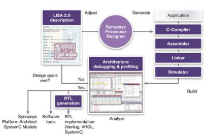
Figure 1 : Processor Designer Infrastructure
As shown in Figure 1, PD automatically generates a simulation model, software programming and debugging-tools, as well as synthesizable RTL. The automatically generated models and RTL feed seamlessly into RTL synthesis, RTL simulation, FPGA and virtual prototyping flows. A LISA model captures all aspects of the processor core architecture such as storage resources, interfaces, functional units, instruction-set encoding and assembly syntax. Functional units refer to all elements in the processor that contribute to functionality which can be data-processing, program control or interfacing. Functional units are described on a register transfer level using C as an input language. However, in contrast to C based algorithmic synthesis tools, the pipelining of functional units is explicitly described using dedicated language constructs. This way, the designer has full control over the resulting micro-architecture and area vs. performance design trade-offs.
From a LISA description, a full software programming tool chain can be generated. This tool chain comprises a compiler, assembler and linker. At each stage in the design, the hardware and software can be co-analyzed using a debugger that provides architectural as well as software analysis and debug information. The debugger supports various backends such as the automatically generated cycle accurate simulator as well as RTL simulation, FGPA or Virtual Prototypes. The ASIP’s RTL is automatically generated from LISA, including configurable debug logic and interfaces and can be mapped to an RTL simulator or FPGA. As virtual prototyping is becoming increasingly important to mitigate the risk of HW/SW integration errors in complex multi-core system, PD automatically generates SystemC TLM 2.0 compliant virtual prototyping models.
LISA and ASIP Design
A de-blocking filter is a post-processing filter within and video encoder and decoder that removes encoding artifacts which result from block based quantization. With full HD resolution, the de-blocking filter has become a major bottleneck in the critical path of a video encoder and decoder. A well optimized software filter implementation requires still a few hundreds of cycles on a RISC type architecture. However, real time constraints to filter full HD (1900x1088x30fps, 192 filter iterations per macro block) at ~300 Mhz do not allow for more than 5 cycles per filter iteration. Therefore, most de-blocking filter designs are implemented hardwired. However, each video standard requires slightly different variations and heuristics for the filtering process which result in complex design, expensive verification and risky designs.
An ASIP instruction-set, micro-architecture and memory architecture can be derived from a reference implementation as follows, as illustrated by operations for ‘Data Load and Store’.
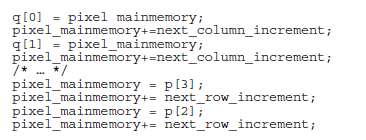
In the reference implementation’s filter core, four â€Q†pixels, are loaded from the pixel storage for one filter iteration. Afterwards, four “P“ pixels are stored to the main memory after a horizontal edge filtering process. The pixels required for vertical edge filtering are organized in a row. The filtered pixels that are available after the horizontal edge filtering are organized in a column. The following example depicts the reference implementation for loading and storing pixels:

Loading and storing of Q and P pixels is always performed with an address increment on the current address. The address increment only changes when switching between vertical and horizontal filtering. This only happens six times (2 Luma + 4 Chroma) per macro-block. Based on this information it can be decided whether the instruction is using implicit or explicit operands. Implicit operands are initialized upon usage in a configuration register and do not have to be encoded in the instruction word. If the operand could potentially change for each call of the instruction, implicit operands would not make sense due to the additional initialization overhead. The following table shows the properties of load/store instructions.
The programmability of the load/store instruction is tailored to the requirements resulting from the de-blocking filter algorithm. There is no requirement to add more flexibility, since this would not result in any benefit. For example, it is not required to store Q pixels or to provide further addressing modes. The ability to initialize an arbitrary address increment is fully sufficient for this algorithm and allows adapting to arbitrary organizations of the pixels in the memory.
Additionally, two registers are required for the storage of the pixel address (PXADDR) and the pixel address increment (PIXINCR). As a next step, the assembly format needs to be defined in order to give the programmer access to this instruction. Since the load instruction and store instruction is implicitly incrementing the pixel address, it is recommended to expose this to the programmer. The following example shows a possible instruction format and instruction sequence :

Here, a pixel is loaded into register Q0 from the pixel memory at the address PXADDR. Then, the register PXADDR is incremented by PXINC. Thus, the next pixel is loaded from the next address.
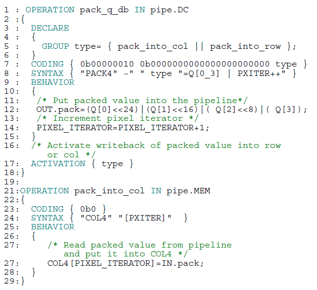
When describing the necessary instructions, architecture descritpion languages like ADL and LISA have found increased popularity. In LISA an instruction is modeled using one or multiple operations. Each operation captures some aspects of the instruction such as coding, syntax and behavior. In order to achieve pipelining, each operation can be assigned to a different pipeline stage. The PACK instruction is modeled using two operations, pack_q_db in stage DC, and pack_into_col (see Example 3, line 1 & 21) which is assigned to stage MEM. The ordering of stages has been declared in a called resource definition in the LISA model (not shown here) along with registers, memories and pins.

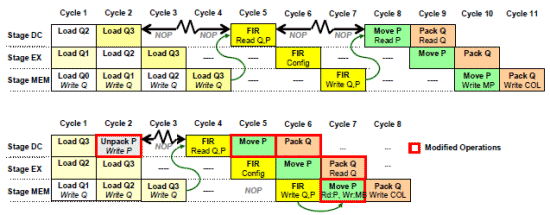
The lines 7 and 8 show the definition of the instruction encoding and assembly syntax. Line 9-15 capture the instruction behavior for the stage DC, here four 8-bit pixels from the Q register file are packed and stored in the pipeline. Line 17 activates a group (choice) of operations modeling the row or column destination register file. The logic of those operations will be generated into the stage MEM, and store the packed value from the pipeline in either the column or row register. The selection is made upon the instruction encoding as described in line 23 for the column register file. The pipeline stage assignment of the individual operations can easily be changed. This allows a late optimization of the pipeline towards an optimal fit (no data dependency delays) for the final instruction sequence as shown in Figure 2.

Figure 2 - Late micro-architecture optimizations
In the example, the instruction MOVE has a dependency on the P register result of the preceding filter instruction FIR, which is only ready in stage MEM. A regular read of the register P in stage DC would result in two expensive delay cycles between the filter and MOVE which have to be filled with NOPs. In order to eliminate the delays, the P register read access done by the MOVE instruction has been shifted to the MEM stage as well. Similar optimizations have been done for the PACK instruction etc. The change can be accomplished with very little effort in a couple of minutes. In contrast, an RTL design would have likely required a major rewrite of the code.
At any stage in the design, programming tools such as compiler, assembler, linker can be generated to map the firmware into binary code for the ASIP. The compiler provides various ways to support complex instructions such as pattern matching, intrinsic or inline assembly. The generated cycle-accurate simulator allows the designer to validate the architecture and firmware from both a functional and performance standpoint. For debugging purposes, a graphical debugger exposes architectural details such as pipeline activity, resource accesses, and unit utilization, along with software performance information. The joint hardware/software analysis enables seamless root cause analysis from software down into the internals of the micro-architecture such as data hazards shown in Figure 2.
The final design performs software pipelining of the load, store and filter operations and fulfills the design goal of less than five cycles for one filter iteration. Software pipelining requires that instructions can be scheduled in parallel by the program. Typically, this needs to be considered very early in the design as it has major impact on the architecture, implementation and software tools. Late changes with such drastic architectural impact are very expensive using manual RTL coding or handwriting tools. Using LISA, those changes only require minimal adaptations to the model. LISA captures the instruction-set in a hierarchical manner, and thus instruction level parallelism is accomplished via tuning this hierarchy.
ASIP Design and Verification
Verification of hardware itself has been a constantly growing problem, with verification efforts reportedly taking up to 70% of the overall project. With the growing importance of software, verification at the hardware-software interface has made verification even more critical.
Specific techniques for verification of the design used in the earlier chapters – a de-blocking filter to remove encoding artifacts in video applications – are outlined in [5], [6] and [7].
The aspects of power optimization and verification are outlined in [5]. For visual verification a display is attached to a ARM Versatile board with an FPGA in a logic tile on the board. The focus of verification is on the comparison of different memory hierarchies and data transfer schemes. To ensure correctness, all of these have to be executed in verification.
A C-model is used in [6] to generate test vectors for verification. The design is verified with eight HDTV (1280x720, 60fps) bit-streams executing 100 frames per bitstream.
The advantages of hardware-based verification are described in more detail in [7]. Video sequences with different sizes (QCIF, CIF and 4CIF) are used to stress different functional requirements. The authors compare verification techniques along different criteria including coltrollability, observability, speed of operationm, cost etc. They arrive at FPGA prototypes as a valid trade-off between speed and cost.
An overview of general verification techniques is presented in [8], comparing methods based on hardware-acceleration, abstraction, assertions, re-use, co-verification and model-based design.
While all of these techniques offer various trade- offs between verification efficiency, cost and execution speed, they all share one basic characteristic. Prior to taping out the design for ASIC implementation, the design’s functionality has to be verified in full using hardware oriented testbenches. This includes all variations of bit-rates, frame sizes etc.
ASIPs offer a very unique, fundamentally different alternative for verification. In custom processor implementation the actual functionality – which drives the majority of the verification effort – is actually not implemented in hardware but instead moves into software. The correctness of the custom processor hardware itself can be verified independent of the function it executes. If multiple custom processor blocks are connected, their interconnect via FIFOs or via memory can be verified statistcally or traces, without executing all funntional permutations on the various processors.
As a result of this separation of structural and functional verification, they also can be separated in time. Specifically, once the actual correctness of the custom processor execution is verified, the implementation can proceed and verification can be done fully in parallel using software. These advantages on verification efficiency are similar to the results achieved with configurable processors as reported in [9].
As execution vehicle, while the hardware implementation is in progress, automatically generated transaction-level models of the custom processor model can be imported into virtual paltforms. Virtual platforms are fully functional software representation of a hardware design that encompass a single- or multi-core SoC, peripheral devices, I/O and board level user interfaces. The achievable simulation speed depends on the level of model abstraction, which also determines the platform’s accuracy. Virtual platforms run on an general-purpose PC or workstation and are detailed enough to execute unmodified production code, including drivers, the OS and applications. As such they are an ideal vehicle for functional verification of the software while the hardware of the custom processor undergoes implementation.
Results
A H.264 de-blocking filter has been designed and verified with a cost of 12 man weeks. The final design consumed 57Kgates and was able to operate at 300Mhz. Next to the data centric de-blocking filter, another ASIP targeting the control dominated motion vector decoding has been developed. As a reference, an existing hardwired motion vector decoder implementation using 45KGates, required 100 cycles per macro-block and 1mW peak power. In contrast, the 50KGate ASIP required 216 cycles per macro-block, 3mW peak power, but was able to serve multi-codes and multi-format including J-PEG, MPEG 1-4, H.264, VC-1 and VP6. The motion vector decoder ASIP supports full-HD (1900x1088@30fps) at 200Mhz. The ASIP has been design within 15 man weeks, including specification and verification time.
Functional verification of the actual H.264 algorithm has been done in software in parallel to the actual hardware implementation. With that, significant schedule improvements can be achieved compared to dedicated, fixed hardware implementation. Outlook
Today’s design automation tools turn ASIPs into a design solution that can be implemented at a competitive cost compared to hardwired logic. Cost refers to the cost of designing as well as the cost of the verification. In contrast to hardwired logic, ASIPs provide flexibility which allows longer and broader use of the design in the market. In addition, functional verification can be separated from hardware verification, allowing significant schedule improvements by parallelizing software verification and hardware implementation.
Moreover, ASIPs mitigate design risks. Complexity is shifted from silicon into software which can be changed even if silicon is at hand. ASIP design automation tool suites, such as the Synopsys Processor Designer, eliminate the software tool creation overhead that is introduced by changing from hardwired to programmable solutions.
References
[1] Norbert When, “An Outer Modem ASIP for Software Defined Radioâ€, MPSoC’08, Chateau St. Gerlach, Netherlands, June 2008
[2] Schliebusch et al., "Architecture Implementation Using the Machine Description Language LISA", Proceedings of the ASPDAC/VLSI Design, Bangalore, India, Jan 2002.
[3] Synopsys Inc., Synopsys Processor Designer, http://www.synopsys.com/Tools/SLD/ProcessorDev/Pages/default.aspx
[4] Schliebusch et al., "Architecture Implementation Using the Machine Description Language LISA", Proceedings of the ASPDAC/VLSI Design, India, Jan 2002
[5] A Low Power Implementation of H.264 Adaptive Deblocking Filter Algorithm, Parlak, M.; Hamzaoglu, I.; Second NASA/ESA Conference on Adaptive Hardware and Systems, 2007, AHS 2007
[6] An implemented architecture of deblocking filter for H.264/AVC, Bin Sheng; Wen Gao; Di Wu ; International Conference on Image Processing, 2004, ICIP '04, 2004
[7] Basavaraj Mudigoudar,†FPGA Prototyping for fast and efficient verification of ASIC H.264 decoderâ€, The University of Texas at Arlington, May 2006
[8] Study of various ways to optimize ASIC design cycle timings, Nirav R. Parmar, Vrushank M. Shah, EHAC'10 Proceedings of the 9th WSEAS international conference on Electronics, hardware, wireless and optical communications
[9] Epson’s Breakthrough REALOID Printer SOC Powered by Multiple Xtensa Processors, Tensilica, http://www.tensilica.com/markets/customer-gallery/printers-scanners/epson-printers.htm
