Jose Simon, Deepu K. Krishnan, S. Krishnakumar Rao, Biju C. Oommen, R. Ravindrakumar
Centre for Development of Advanced Computing
Abstract:
This paper discusses a method to design an SD Host Controller IP Core that can be implemented on FPGAs. FPGAs are being widely deployed in various applications including industrial, commercial and military applications. Secure Digital is the most widely used portable memory standard. Its ultra-compact and rugged architecture, simple interface, high security, low power consumption, reliable operation and interoperability have made it the de-facto solution for portable storage. The IP Core is designed in accordance with SD Host Controller Specification 3.0 and implements many advanced features. The IP Core is developed, implemented and tested and the performance obtained matches industry standards.
1. INTRODUCTION
The need for portable digital storage in embedded systems is increasing ever rapidly. The Secure Digital technology, though developed just 12 years ago, have got overwhelming support from the industry and pushed all its competitors like Compact Flash, Smart Media, Multimedia Card etc backward. SD Cards are now being used in over 8000 products including digital cameras, mobile phones, GPS receivers and other hand held devices [1].
An SD Host Controller IP Core enables an FPGA based embedded system to access an SD card through the I/O pins of FPGA. The IP Core can be easily integrated with the rest of the system.
2. SECURE DIGITAL TECHNOLOGY
2.1 Overview
Secure digital is a non-volatile memory card format developed and managed by Secure Digital Association. SD Card is a semiconductor flash based memory device which is well known for its simple interface, high bandwidth, low cost, greater security, low power etc. The SD Card can easily be connected to a personal computer also.
SD Host Controller implements the SD Host Controller standard specification version 3.0. It enables the host to access SD Devices such as SD Memory Cards, SDIO devices, SD Combo devices etc.
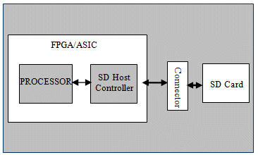
The SD Protocol operates a Master-Slave communication model. It employs a command-response mechanism. Commands are always initiated by the Host Controller and responded to by the Card. The Host Controller has two interfaces: the System side interface and the SD Bus interface. The Host Controller assumes that both these interfaces are asynchronous. The Host Driver is on system bus time and the SD Card is on SD Bus time. The Host Controller will synchronize signals to communicate between these interfaces [2].

Fig.1. System Architecture
2.2 SD Bus Interface
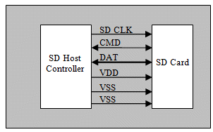
SD Bus Interface is an advanced 9-pin bus consisting of one clock line, one bi-directional command line, 4 bi-directional data line and 3 power lines. The bus is designated to operate at a maximum operating frequency of 200MHz depending on the capabilities of the Card.
The Data transfers to and from the SD Memory Card are done in blocks. Data blocks are always succeeded by CRC bits. Single and Multiple block operations are defined. Data can be transferred using single or multiple data lines [3].

Fig.2. SD Bus Interface.
3. DESIGN OF SD HOST CONTROLLER
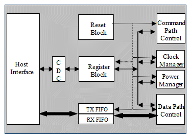
The SD Host Controller is fully compliant to SD Host Controller Specification version 3.0 and Physical Layer Specification version 3.01. The standard register set is implemented. Internal FIFOs are provided for temporary buffering of ingress and egress data. The Host Processor accesses the various registers and FIFOs in the Host Controller to transfer data between Host and SD Card. Every data transfer is preceded by corresponding command and response. Command is send by the Host Controller to the Card and Response is send back by the Card to the Host Controller. The block diagram of Host Controller is given in Figure 3.

Fig.3. SD Host Controller IP Core Block Diagram
3.1 Command Path Control
This block deals with the process of command transmission and response reception. All commands are 48 bits long with a 6 bit command index, 32-bit argument and a 7-bit CRC field. Each command is preceded by a start bit ‘0’ and a transmission bit ‘1’ and succeeded by an end bit ‘1’.
The Host Processor writes argument into the argument register and command into the command register in the Host Controller. The command path control block then forms a frame with the given data, finds and attaches a 7-bit checksum and transmits along the one bit wide command line to the card.
Having received a command, the card checks for errors and replies with a response with the same index field. The transmission field will be ‘0’ and the argument field will contain status of previous command. The command path control block checks the response for CRC or any other error and stores in the Response register.
3.2 Data Path Control
The data path control block manages the process of writing and reading data between Host and SD Card. Transmit and receive buffers help in temporary buffering. Data is accessed as a block, in an SD card. In SDSC cards, the block size is not fixed, but default size is 512 bytes. In SDHC and SDXC, the block size is fixed 512 bytes. Every data block is preceded by a start bit ‘0’ and succeeded by 16-bit CRC and stop bit ‘1’.
For write and read, the SD Host Controller supports both single block and multiple block access. In single block read and write, only one block of data is transferred with each read or write command. In multiple block access method, infinite number of blocks can be transferred by sending one command. For stopping a multiple block operation, a transmission stop command (CMD12) is sent by the Host Controller.
To perform a write operation, the data to be transferred is written to the Transmit FIFO through the Host Interface and data write command is issued. When the write command is sent by the Command Path Control block, the Data path control block sends the data along with CRC and end bit. The SD Card will check the received data for any errors and will give back a 3-bit CRC status indicating whether the data is successfully written or not.
To perform a read operation, the read command is sent. After receiving the read command, if no error is found, the SD Card sends the requested data through the data lines. It will be checked for any errors and stored in the Receive FIFO. The Host Processor can read it through the Host Interface.
3.3 Register Block
The Register Block stores all the configuration and status information of the SD Host Controller. The standard register set described in [2] viz, SD Command Generation register, Response register, Buffer Port, Configuration and interrupt Control register are implemented. Since the IP Core is a single slot controller, only one register set is implemented.
3.4 Host Interface
The Host Interface is a 32-bit general purpose processor interface consisting of host clock, read enable, write enable, address and data ports. All the registers in the Register Block and Receive and Transmit FIFOs are accessed by the Host through the Host Interface.
3.5 Clock Manager Block
The Clock Manager block generates various clock frequencies for several modes of data transfer in the SD Host Controller. The initialization is carried out at 300KHz. Once initialized, the frequency is switched either to 25MHz, 50MHz, 100MHz or 200MHz depending on the mode of operation. The clock switching can be performed through the clock control register of the register block.
3.6 Power Manager Block
The Power Manger block controls the signal voltage level of the SD Bus Interface. It also provides the Host with the capability to switch on and off power to the SD Card to re-initialize it
3.7 Clock Domain Crossing Block
The Clock Domain Crossing Block enables the Host Interface to be asynchronous to the SD Bus Interface. Advance clock domain crossing circuit is implemented to enable this. It confirms data integrity when signals are crossing clock domains.
3.8 Reset
The Reset Block brings all modules in the SD Host Controller to a reset state in the event of a software or hardware reset or during error recovery.
3.9 Transmit and Receive FIFO
These FIFOs are used for temporary buffering of transmit and receive data. The data to be written to the SD Card is buffered in to the Transmit FIFO. The IP Core reads this data, frames it and sends it along the SD Bus to the SD Card. Likewise, the data read from the SD Card will be available in the Receive FIFO when read operation is complete.
4. OPERATION
There are two modes of operation defined for SD Memory cards.
4.1 Card Identification Mode
In this mode the host initializes the card, the goal of this mode is to validate if the card and host are compatible. Also the host will know what kind of card it is communicating with -SD, SDHC, SDIO or MMC card. The difference between the cards is in how they respond to the commands in the identification mode. All the communication in this mode is performed on the CMD line. The initialization process starts by holding the CMD line high for 74 clock cycles. Then the card is reset by sending reset command (CMD0) which takes the card to the idle state. In the next step, to validate the interface condition, the host sends its operating voltage range to the card through CMD8. The card responds only if it is specification 2.0 compatible and if the operating voltage is valid for the card. If no response is received, then host knows that it is either a 1.0 card or an operation condition mismatch. However, if a response is received the host knows that it is a 2.0 card and additional features can be enabled. A received response is validated with CRC check and bit matching; an invalid response will put the card in inactive state. Next command (ACMD41) provides SD Memory Host with a mechanism to identify and reject cards which do not match the VDD voltage range desired by the host. When a response of the operation condition is received, it checks for a busy bit in the response data field. If the busy is set, the operation command is resent until the busy bit is cleared, then the host knows the card has finished its start-up operations. The content of the response also indicates if a card has compatible operation conditions. The SDHC or SDXC cards reply with a CCS bit in the response, indicating it is a high capacity card. A voltage switching sequence (CMD11) is done if required to switch to higher bus speeds. [3]

Fig.4. SD Card Initialization Flow Chart
The host then reads the unique Card Identification register. The final command (CMD3) in the initialization sequence is the request for Relative Card Address (RCA) which is the address of the card, used when addressing cards in the data mode. Clock frequency shall be 100KHz to 400KHz during initialization sequence.
4.2 Data Transfer Mode
After the identification mode the card will be in the standby state. To set the card to transfer state one additional command (CMD7) containing the RCA number is sent, card with matching RCA number will then be put in data transfer mode. Before transmitting data some parameters are set. The data width can be set to 1 or 4 bit (ACMD6) and the block length that can be set to a value between 1 and 2048 (fixed to 512 for SDHC or SDXC card) [3].
5. IMPLEMENTATION AND TESTING
The SD Host Controller IP Core was developed in Verilog HDL and implemented in a Xilinx Spartan 6 XC6SLX150TFGG676 FPGA based development board. It consumed 1076 slices (2600 Flip-Flops & 2000 LUTs) of the device.
The SD Host Controller IP was integrated with a 32-bit RISC processor, UART IP and Memory. SD Cards from various manufacturers of different capacity from 2 GB to 16 GB were used for testing.
A firmware was developed using ‘C’ to implement FAT32/FAT16. The firmware could select FAT32/FAT16 depending on the card capacity. It had capabilities to format the SD Card, creating or deleting a file or folder, reading or writing a file or folder, renaming a file or folder and setting volume label. A file could be saved into the SD Card by sending it through UART from a PC’s HyperTerminal. It could also be retrieved through HyperTerminal.
6. PERFORMANCE
The following table shows the effective bandwidth obtained while writing and reading raw data using multiple block commands with SD Clock at 24MHz.
Table 1. EFFECTIVE BANDWIDTH OBTAINED
| Transfer | Card | No. of Blocks | Time (S) | Effective BW (MB/s) |
| Read | SANDISC 2GB | 65535 | 3.65 | 9.19 |
| Write | SANDISC 2GB | 65535 | 4.33 | 7.74 |
7. CONCLUSION
The SD Host Controller IP Core was implemented in Xilinx Spartan 6 FPGA and was tested for effective bandwidth. Read and write speeds of 9.19MB/s and 7.74MB/s were obtained respectively without compromising data integrity. SD Host Controller IP Core can be integrated with standard processor cores and can be used in a wide range of FPGA and ASIC based applications which require high speed portable storage of data including surveillance, data archival etc.
8. REFERENCES
[1] Global Industry Analysts,Inc; “Secure Digital Memory Cards: A Global Strategic Business Report†, July 2012.
[2] SD Specification Part A2; SD Host Controller Standard Specification, Version 3.00, 2010.
[3] SD Specification Part 1; Physical Layer Specification, Version 3.01, 2010.
