Arzu Datli, Umut Eksi, Gokhan Isik (Ericsson)
Abstract
This paper aims to share practical experience regarding building a power-optimized clock tree, determining the optimum targets for clock tree synthesis (CTS) and monitoring the quality of results (QoR) along the way. The experiments that will be presented were conducted on a mixed-mode design, which has multiple power domains with 100K+ registers, and which was intended for a 55nm CMOS technology node. The methodology presented here resulted in clock tree power savings of up to 20% according to simulation results.
Introduction
Clock tree synthesis (CTS) is a critical step in the physical implementation flow. An optimized clock tree (CT) can help avoid serious issues (excessive power consumption, routing congestion, elongated timing closure phase) further down the flow [1]. The need for further optimizing the clock tree has emerged in one of the customer projects when it was realized that the clock tree constituted almost 75% of overall power in a certain mode of operation. Several experiments were conducted to diagnose and treat this issue. At the end of project, a reduction of approximately 20% in clock tree power was achieved.
There are many factors that affect the way a clock tree is built therefore designers often have to run many experiments in an attempt to optimize the clock tree. Clock gating structures, CTS targets, clock library cell types and even placement of spare cells have direct impact on the quality of a clock tree. Monitoring the QoR can become a challenge for CTS experiments that generate excessive amounts of data. Key Metrics
A set of key metrics (in Tables 1 and 2) were identified to be monitored in order to analyze and compare the results of several experiments as well as to detect and correct any deviation from design targets at any point in time. A number of experiments need to be designed and performed in order to find the optimal CTS targets.
| Parameter | Remarks |
| CT power | Direct indicator of CT power Maximum clock insertion delay (ID) Indicator of CT depth |
| CT area | Indicator of CT power and area |
| CT Cell Count | Indicator of CT power and area |
| Transition times on clock nets | Indicator of CT and timing quality |
| Ratio of high-leakage standard cells | Indicator of timing quality and power |
Table 1: Power-related key parameters
| Parameter | Remarks |
| Global/Local Clock Skew | Indicator of how well clock sync points are balanced |
| Worst/Total Negative Slack | Indicator of timing quality |
| Global Routing Congestion | Indicator of routability |
Table 2: Secondary set of key parameters
Experiments
Slew Rate
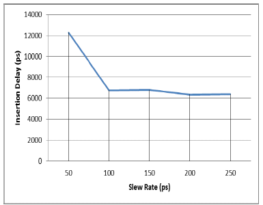
Figure 1: Slew Rate v.s. Insertion Delay
Slew Rate (SR) target has a direct impact on the resulting clock insertion delay as shown in Figure 1. It should be noted that insertion delay degrades drastically if SR target is forced below a certain threshold (somewhere between 50 and 100 ps in this case). The implications of target SR on other key metrics are shown in Figures 2, 3, 4 and 5.
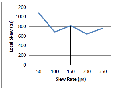
Figure 2: Slew Rate v.s. Local Skew
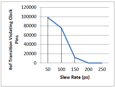
Figure 3: Slew Rate v.s. Number of Transition Time Violations
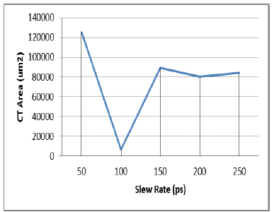
Figure 4: Slew Rate v.s. CT Area
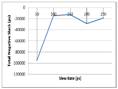
Figure 5: Slew Rate v.s. TNS
Multi-Vt Clock Cells
It is not advisable to mix cells with different threshold voltages (HVT/SVT/LVT/etc…) when building the clock trees. Hence, it is important to pick the right threshold voltage for the clock tree cells in the design. The higher the threshold voltage, the higher becomes the insertion delays and skew however the lower becomes the power. This critical decision should be based on a number of experiments and project targets. The results of experiments for different key metrics are shown in Figures 6-9.
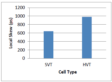
Figure 6: Vt v.s. Local skew
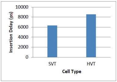
Figure 7: Vt v.s. ID
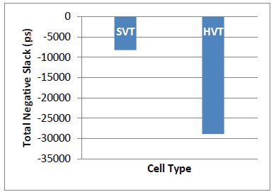
Figure 8: Vt v.s. TNS
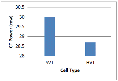
Figure 9: Vt v.s. CT Power
Standard-Vt clock cells are shown to offer more advantages compared to their high-Vt counterparts with improved ID, local skew. WNS/TNS and signal transition times.
Clustering and Grouping
Clustering (regioning) of certain critical non-buffer cells (multiplexers, flip-flops in clock, etc…) in the physical design flow can help reduce clock tree power especially if they are located upstream, i.e. closer to the clock roots (Figure 10). The ports of such cells are very likely to switch unconditionally. Smart clustering will prevent unnecessary buffering among these cells and hence will minimize the chances of having unnecessary high-frequency toggling and power dissipation.
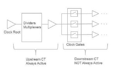
Figure 10: Clock logic can be clustered/grouped to improve upstream/downstream CT power respectively.
Optimal grouping clock tree sinks for clock gating during both the RTL design and synthesis stages offer significant advantages for power saving. The grouping and clock gating that can be coded manually by the RTL designer who knows the architecture and typical application scenarios for the device is the most critical part that contributes most to the power savings. The power optimization via automatic clock gate (ACG) insertion in the logic synthesis tools is also very crucial. The effectiveness of ACG can be tailored through several options in the tool therefore it is good practice to run several experiments during the synthesis step to find the optimal set of parameters.
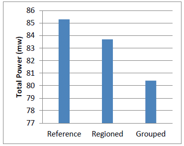
Figure 11: Effect of Clustering and Grouping on Total Power
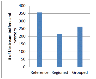
Figure 12: Effect of Clustering and Grouping on Up- and Down-stream CT cells
Basically clustering the clock gating cells improves upstream CT power and grouping the clock gating cells improves the downstream CT power. It has been observed that most of the clock tree power is contributed by the downstream CT. Figures 11 and 12 show the data for the related experiments.
Set of Allowable Cells
It has also been shown to be a good idea to limit the drive strengths of allowable cells to a certain range when building the clock tree. Allowing cells with drive strength that lie on the higher end of the scale may result in improved ID. However, they are more likely to cause EM, IR drop or cross-talk issues later in the flow. On the other hand, having cells with weak drive may result in degraded insertion delay and cross-talk vulnerability. Similarly, determining the optimal set of drive strength can only be possible by running several experiments.
Under identical conditions with the previous experiment (clustering and grouping the clock gating cells) prohibiting the use of clock tree cells with certain threshold results in a degraded performance in terms of power (-6%) and area (-7%).
Spare Cells
The way spare cells are placed and connected in the design can have adverse effects on the quality of the clock tree if special cares are not taken. There are a couple of options when it comes to placing spare cells on a chip. If the spare cells are inserted before P&R into certain modules in the design hierarchy, the common option is to treat them as regular cells and leave it to the P&R tool to place them automatically based on their hierarchical position and their connectivity just like any other cell in the design. If spare cell insertion is performed during P&R, one option would be to have the spare cells placed semi-randomly, that is by trying to maintain a certain density across the die.
The connectivity among the spare cells plays an important role as well. If there are spare clock tree buffers/inverters that are hard-wired to spare flip-flops, the way these cells are placed becomes critically important. The P&R flow should make sure that spare clock buffers/inverters and associated spare flip-flops are placed close to each other. Randomization in placement of spare cells might cause these cells to get placed too far from each other and this may in turn cause excessive increase in the ID of the associated clocks.
Standalone CTS Tool
It is possible to achieve a reduction of up to %20 in clock tree power if a standalone CTS tool is used in the flow. In this approach, a regular P&R flow with integrated CTS capability is modified in such a way that the design is exported after placement (and any associated optimization steps) and fed into the standalone tool that offers a specialized CTS engine with potentially higher quality. The outcome of the tool is supposed to be conveniently imported into the regular P&R tool after CTS is completed.
The quality of routing and CTS is also reflected on the number of design rule violations (maximum transition times, shorts, etc…) and timing (less number of violations due to better skew balancing and less variation) as shown in Figure 13. The comparison of power savings in two different power scenarios are illustrated in Figure 14. On the other hand, the part in which the constraints between the P&R tool and the CTS tool were translated and transferred was not as straightforward as expected. This process requires extra precautions to be taken to go through smoothly.
Firstly, special tool-specific attributes (such as “don’t touch”) on nets or cells, constraints, definitions that are coded in the command set of one tool have to be translated for the other. Several issues such as net/cell name mismatches due to different hierarchical naming conventions, clock nets violating maximum length or minimum drive constraints or unrecognized new clock ports that were created by the CTS tool. Unless an officially verified and supported flow between the two tools exists, all these steps should be well-scripted so that iterating between the tools is fast, smooth and dependable with minimal need for manual intervention.
It is also highly recommended to run a capacitance correlation study between the different extraction engines of the two tools to ensure that timing optimizations performed by the CTS tools can be valid and reflected on to the main P&R tool when the design with CT is imported back.
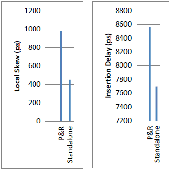
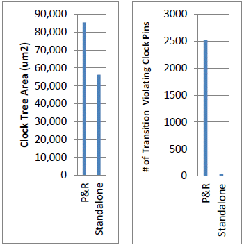
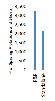
Figure 13: Comparison of key metrics using P&R and standalone CTS tools
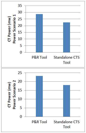
Figure 14: Power Savings in 2 Different Power Scenarios
Conclusion
It is recommended to allocate sufficient time in the project plans for CTS experiments as it is an investment for improved overall lead times and quality. The key metrics should be closely monitored through the experiments to determine optimum targets for CTS. Involving a standalone CTS tool in the physical design flow can be considered provided that the associated risks are well-understood and planned for in advance.
References
[1] Synopsys Low Power Methodology Manual for System-On-Chip Design (Springer PDF Edition 071001)
