Yasha Jyothi M Shirur, Veena S Chakravarthi, Gourav Thakur (BNM Institute of Technology)
Abstract
Today's complex VLSI SOC solutions demand low power processors. Synchronous processors which consume more than 40 % of power in clock circuitry are being conveniently replaced by low power delay-insensitive (DI) asynchronous Processor modules/cores. In this paper, power, area performance parameters of 8-bit pipelined asynchronous processor is measured and compared over similar feature synchronous processor. The Asynchronous processor supports 28 Arithmetic and Logical Instructions. The module to module hand shaking is performed using 2 phase mousetrap pipelining. The implemented processor has given dynamic power advantage of 49% over synchronous processor. The design is a synthesizable core which can be extended to complex RISC or DSP architectures by integrating MAC (Multiplier and Accumulator) core and hence is a right choice for any MPSOC designs.
Index Terms
Multi Processor System on Chip [MPSoC], Delay insensitive [DI], 2 phase Mouse trap Pipeline.
I. INTRODUCTION
Most of the System on Chip (SoC)s today are synchronous and operates at a single clock frequency or its derivative. In synchronous processors more than 40% of the power is consumed by clock, which is used to synchronize the whole processor. The complexity of clock routing to various parts of the processor is increasing due to clock skew issues. Major challenges in such designs are clock distribution, timing closure, scaling up of clock frequencies, power consumption, and reusability. As the trend for smaller feature and higher speed continue, clock management and power dissipation increases affecting design performance. The power inefficiencies of clocked circuit¡¦s are emerging as the dominant factor hindering increased performance.
The elimination of the clock results in reduced die size as well as reduced design complexity. In synchronous processors each stage needs to be optimized and the speed depends on the slowest stage. In asynchronous processors each optimized element can speed up the processor. Due to ever increasing need for high performance, low power systems, have renewed interest in asynchronous digital design.
The delay-insensitive (DI) asynchronous modules/ cores have a number of advantages, especially in SoC, including reduced crosstalk between analog and digital circuits, ease of integrating multi-rate circuits, and ease of component reuse.
In asynchronous designs synchronization is performed through request and acknowledge lines, rather than through global clock. So that, modules can communicates using asynchronous handshake protocols. The number of handshake components determines the system complexity. In future, complex SoC designs will be predominantly asynchronous as predicted by ITRS 2011[3]; the asynchronous part being driven by handshake Signals.
It is extremely important for designers to introduce asynchronous paradigms to make them more marketable and more prepared for the challenges faced by the digital design community in the years to come. Currently, companies such as ARM, Phillips, Intel, and others are incorporating asynchronous logic into some of their products using their own proprietary tools [1]. ITRS roadmap 2011 also reports that numbers of asynchronous blocks are going to be more compared to that of synchronous blocks in any complicated SoC. In this paper 8 bit pipelined asynchronous processor is implemented.
II. PIPELINE IMPLEMENTATION METHODOLOGY
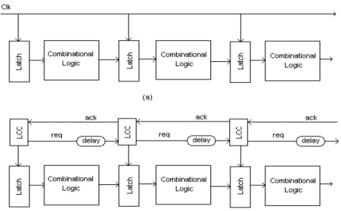
The aim is to design 8-bit pipelined asynchronous processors. The operation of pipeline is explained with the help of a diagram shown in Figure 1.

Figure-I (a) Synchronous pipeline and (b) Asynchronous pipeline
If Nth instruction is in executing mode then N+1 instruction is being fetched and N-1 instruction's results are being written back. Specialized hardware is required in slower stages to increase the operating frequency of the synchronous pipelined processor, whereas this requirement can be eliminated in asynchronous pipelined processors. The execution time of the asynchronous processors is dependent on the average execution time of each block whereas in synchronous processors the execution time is mostly dependent on the worst case delay of the slowest block [1].
In synchronous pipelined processors each stage should perform operation in a given lock time irrespective of status of the next or previous stages, whereas in asynchronous pipelined processors, the condition to process data in the Nth stage is that the N+1 stage should have acknowledged the previous request and there is a new request from the N-1 stage. This can result in decentralized and less complex control unit. Figure 1 (a) shows the synchronous pipeline where clock is connected to all the latches and the clock frequency depends on the worst case execution delay of the slowest combinational logic. Figure 1 (b) shows the asynchronous pipeline where request and acknowledge signals are used to transfer data between two stages. LCC are the latch control circuitry which enable the latches whenever acknowledge is received from the next stage i.e. given data is captured by the next stage.
III ASYNCHRONOUS HANDSHAKING PROTOCOLS
The asynchronous protocol used in this processor is 2-phase handshaking. In the 2-phase handshaking it requires 2 transitions to complete one transition. As seen in Figure-2 the request signal is from transmitter to receiver, and the acknowledge signal is from receiver to the sender.

Figure-1: Basic Asynchronous Communication Protocols
In 2-phase protocol initially both request and acknowledge signals are assumed to be in reset condition, a transition on the request signal indicates that the data is ready and the same transition on the acknowledge signal indicates that the data is captured [1].
2-phase handshaking is also referred as Mouse trap Pipeline. This pipeline is chosen because of its simplicity. To design its control and data latches, it has few complex signals [1]. The control consists of only a two input XNOR gate and the data consists of level triggered latches as shown in Figure 3.
Initially all the requests and acknowledges are in the same state. A transition on the req0 produces a same transition on the ack1 after one gate delay. The req0 is delayed and applied to the second stage as req1; the delay depends on the worst case combinational delay of that stage.

Figure-3: Mousetrap pipeline [1][5]
IV ASYNCHRONOUS PROCESSOR IMPLEMENTATION:
The design implementation includes performance analysis of 8-bit Asynchronous Pipelined Processor; the performance is compared against Synchronous Pipelined Processor with the similar instruction set and functionality. The design complexity of each processor is around 10K gates. Each processor supports 28 typical instructions. The pipeline style used for asynchronous processor is Mousetrap pipeline which uses a two phase handshaking protocol.
The processing of instructions is divided into 3 different stages like Instruction Fetch (IF), Execution (EXE), and Register Writeback (WB) which is similar to that of RISC DLX Processor. The pipelining of the instruction fetch is as shown in Figure 4. The specification of the 8 bit Pipelined Asynchronous Processor is depicted in Table 1.

Figure-4 Three3 Cycle Pipeline Instruction Fetch

Table 1: Specifications of Pipelined Asynchronous Processor
Functional specifications of the processors:
- Addressing capability 64k.
- 4 Ports, Port A is multiplexed Address and Data, Port C only for Address, Port B and Port D output ports.
- Processor would execute 28 typical Instructions.
- 256 internal registers with address from 00h to FFh, Accumulator ¡VA specifies the address F0h of the register.
- Two program status flags CARRY and ZERO.
- Asynchronous processor designed with Mousetrap Pipeline style with three intermediate stages.
The implemented processor is able to perform arithmetic operations like ADD and SUBTRACT, logical operations like AND, OR, XOR and COMPLIMENT, and branching instructions like JUMP operations unconditional or conditional depending on the status of carry flag. The instruction length varies in size from 1 byte to 4 bytes long. The interface unit first fetches the OPCODE and then fetches remaining operands depending on the OPCODE. The interface unit of the processor consists of the Program Counter (PC); this unit fetches the instructions and operands from Port A. The OPCODE and Operands are then propagated through the pipeline for execution.
There are three instruction formats in this processor R-type, I-type, and J-type. All instruction formats must specify an OPCODE; however, the other information in the instruction varies by format. R-type (register) instructions specify three registers in the instruction - two source registers and one destination register. I-type (immediate) instructions specify one source register, one destination register, and a 16-bit immediate value that is sign-extended to 32 bits before it's used. J-type (jump) instructions consist of just the OPCODE and a 26 bit operand, which is used to calculate the destination address. The instruction format is as shown in Table 2.

Table 2: Instruction Format
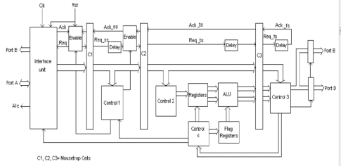
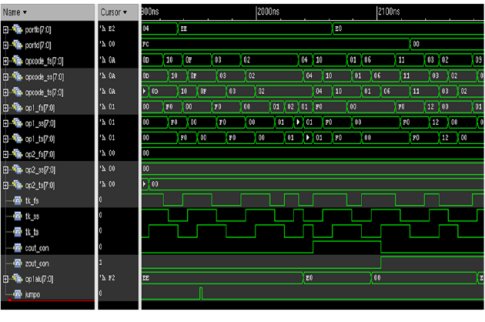
The block diagram of the 8bit pipelined asynchronous Processor is as shown in Figure 5 and the timing diagram is depicted in Figure 6.

Figure-5: 8 bit Asynchronous Pipeline Processor

Figure-6: Timing diagram of Asynchronous Processor
V. FUNCTIONALITY VERIFICATION
Several test scenarios are considered to check the functionality of the processor.
CASE-1: The processor is interfaced with ROM consisting of some instructions test scenario is depicted in Figure 7 and timing diagram is as shown Figure 8. The Interface unit test scenario consists of two 8bit tristate latches. One latch is to hold the address from Port A. The other latch is to hold data from the ROM output.

Figure-8 Interface Unit Test Scenario
The timing diagram shown in Figure 9 is an example of three byte instruction which would consists of one OPCODE and two addresses.

Figure-9 Timing Diagram of Interface Unit
CASE-2: The Read and Operate unit performs reading from the sources and performing operation on them and then routing them to proper destination by generating control and enable signals to register bank, PSW, ALU and Multiplexer. The details block diagram is as shown in Figure 10.

Figure- 10 Block Diagram of Read and Operate Unit
The timing diagram of read and operate unit is as shown in Figure 11.

Figure-11 Timing Diagram of Read and Operate Unit
CASE-3: The Write back unit generates control to store results, accurate control signals to register bank like we1, we2 etc, to PSW like czwrite, and also does decisions about branching depending on the flag status. It also generates control signals to write onto the Port B and Port D, controls demultiplexer to route data to register bank or to the output ports. The block diagram of write back unit is as shown in Figure 12

Figure- 12 Block Diagram of Write Back Unit
The timing diagram of write back unit is depicted in Figure 13

Figure-13 Timing Diagram of Write back Unit
CASE-4: The pipeline stalling mechanism is required in order to overcome data hazards and in case of branch decision condition. This unit is designed and is as shown in Figure 14

Figure-14: Pipeline stalling mechanism
The critical test scenarios for any of the asynchronous processor are considered and discussed. The implemented processor is capable to support any such conditions. Many other scenarios like data hazard detection and branch detection are also considered to verify the functionality of the processor by giving appropriate conditions.
VI. RESULTS AND DISCUSSIONS
Both the 8 bit pipelined asynchronous processor and synchronous processor designed in Verilog and simulated to check the functionality using NCSIM simulator from Cadence. The synthesis reports for power and area are taken from Cadence Encounter Tool and RTL Complier to do perfromance analysis. Some of the simulation results obtained for the different test scenarios are shown in Figure 16, through 20.

Figure-16 Simulation Result of Read and Operate Unit of Asynchronous Processor

Figure- 17 Simulation Result of Write Back Unit of Asynchronous Processor

Figure 18 Simulation Result of Interface Unit

Figure- 19 Simulation Result of Asynchronous Processor

Figure-20 Simulation Result of Synchronous Processor
The Synthesis report obtained is summarized in the form of a table which is depicted in Table 3

Table 3 Area and power comparison of two processors
From the above table in can be concluded that lot of dynamic power can be reduced if the asynchronous processor of same feature is designed.
VII. CONCLUSION AND FUTURE SCOPE
The 8 bit pipelined Asynchronous pipelined processor and Synchronous pipelined processor is designed and verified. The design is coded in Verilog and simulated in NCSIM simulator. Both the designs are synthesized in Encounter RTL Compiler and the results are compared.
The Salient Features of the processors are
- The Asynchronous processor complexity is 10445 gates.
- The Synchronous processor complexity is 9465 gates.
- Dynamic power consumption of Asynchronous processor is 8.5£gW.
- Dynamic power consumption of Synchronous processor is 47.6£gW.
The results show 82% reduction in dynamic power in Asynchronous Processor. Simulation results show that the execution time advantage in the Asynchronous Processor as the number of Data hazards increases in the instructions.
Future Scope
In current scenario where complex computing devices are required in which case processors will have many supporting blocks like scratchpad, internal instruction and data cache, interrupt processor, bridges, instructions with DSP capabilities etc. The complexity is further increased when multiple of such processors are used in MPSOCs. When a dynamic power advantage of 82% is achieved in simple processor as in this case, it is for sure to get more power advantage in MPSoC scenario. However the effect of it in with DFT, timing closure etc need to be kept in mind when implementing asynchronous processors in MPSoCs.
ACKNOWLEDGMENT
The authors wish to acknowledge BNMIT Management for supporting this work. .
REFERENCES
1. Steven M. Nowick and Montek Singh, "High-Performance Asynchronous Pipelines: An Overview", IEEE Design & Test of Computers , vol. 28 , pp. 8 - 22, Sept.-Oct. 2011
2. Meng-Chou Chang and Da-SenShiau, "Design of an Asynchronous Pipelined Processor", ICCCAS , pp. 1093 ¡V 1096,2008
3. S.B. Furber, P. Day, J.D. Garside, N.C. Paver and J.V. Woods, ¡§AMULET1: a Micropipelined ARM¡¨, CMPCON-1994 , pp. 476 - 485.
4. Werner T., Akella V., "Asynchronous Processor Survey". Computer Volume: 30, Issue: 11 Publication Year: 1997, Page(s): 67 - 76.
5. Montek Singh and Steven M. Nowick, "MOUSETRAP: High-Speed Transition-Signaling Asynchronous Pipelines" IEEE Trans. Very Large Scale Integration (VLSI) Systems, vol. 15, no. 6, 2007, pp. 684-698.
6. Jurj Silc and Borut Robic, "Asynchronous Microprocessors" Informatica journal 23, 1999, pp. 239-247.
7. Raanan Zacher and Raz Kivelevich-Carmi, "The Design and Implementation of an Asynchronous RISC Processor" VLSI Laboratory Department of Electrical Engineering Technion-IIT.
8. Scott Hauck, "Asynchronous Design Methodologies: An Overview" Proceedings of the IEEE, Vol. 83, No. 1, pp. 69-93, January, 1995.
9. I.E. Sutherland, "Micropipelines" Comm. ACM, vol. 32, no. 6, 1989, pp. 720-738.
10. Furber S.B., Garside J.D., Gilbert D.A.,"AMULET3: a high-performance self-timed ARM microprocessor" ICCD, Publication Year: 1998, pp: 247 - 252.
11. Furber S.B, Garside J.D. , Riocreux P., Temple S., Day P., Jianwei Liu, Paver N.C., "AMULET2e: an asynchronous embedded controller", Proceedings of the IEEE Volume: 87 ,pp: 243 - 256.
