By Chris Menkus and Scott Lewis (City Semiconductor, Inc.)
Overview
Commercial time-interleaved ADCs have been available since the early 2000’s. Since then the number of academic and industry-sponsored articles showing the advantages of interleaving has been steadily increasing.
Interleaving provides clear advantages in terms of power and speed. This is mainly due to the square-law dependence between current and bandwidth in analog signal paths, and secondly because we can take better advantage of clever architectural innovations with lower-speed circuits.
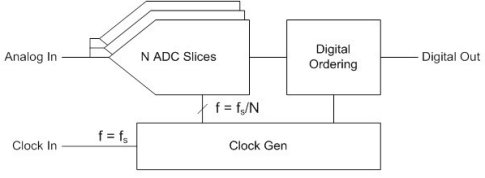
Figure 1: Basic block diagram of an interleaved ADC
The main challenge of interleaving, of which most people are now aware, is that un-treated mismatch between interleaved units can cause spurs in the output spectrum. The source of this mismatch is usually random variation in the semiconductor processing, and is unavoidable for mid-to-high resolution ADCs. Gain and offset mismatch may be considered as DC effects, while the effects of timing and bandwidth mismatch become worse with higher-frequency analog inputs.

Figure 2. An example gain mismatch waveform and the resulting output spectrum
Various forms of calibration have been proposed to correct these mismatches and reduce the resulting spurs. Gain and offset mismatch correction are the most straightforward, and will be discussed first. A calibration routine may be considered as “foreground” or “background”, depending on whether or not the output data stream is interrupted during processing.
Foreground Calibration
Foreground calibration implies that the converter is taken off-line for a short period of time in order to inject some form of reference signal, or to force circuit blocks into a known state. With the reference applied, the converter output is sensed in order to determine the direction and amount of correction needed. Correction may either be applied through an analog feedback DAC, or as a digital post-processing step. This form of calibration may be considered the most generic, because it does not require a specific type of input signal.
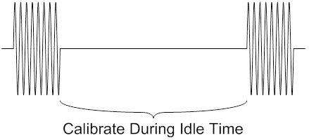
Figure 3:An example of a foreground calibration period
The injected reference signal may be static, for example 0V differential (ie. shorted inputs) to measure differential offsets, or stepped through a range of values to stimulate multiple codes. If desired, the unit quantizer’s linearity may also be measured and improved with a stepped range of input values, but this is another separate topic.
Foreground calibration is useful for applications where the input signal is not known ahead of time or may behave in unpredictable ways.
The drawbacks of foreground calibration include the requirement to tolerate a temporary loss of data while the calibration routine runs. Some applications may be better suited to tolerate this. For example, a transceiver that sends and receives signals on the same I/O pin at different times can calibrate the ADC during the transmit phase. Test & measurement and range finding (eg. LIDAR) equipment are other examples of systems where data is sporadic and there may be a natural down-time for performing repeated calibrations.
Background Calibration
As the name implies, background calibration works in the “background” to sense and correct various sources of mismatch. Its main advantage is that normal output data is not interrupted. Background calibration compensates for drifts due to time, temperature, or supply variation, but puts extra requirements on the input signal. The input must either obey a known statistical behavior, or if it doesn’t, a calibration tone or dithering signal must be added to the signal path and then subtracted out at a later stage.
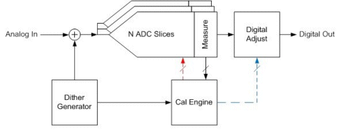
Figure 4: An example of an interleaved ADC with background calibration
The simplest form of background calibration is to rely on the statistical properties of the input signal to exercise the individual interleaved units in a similar-enough way to allow relative comparisons. The unit outputs are then averaged, compared, and their errors extracted. As a simple example, if the analog input is a beat frequency of the sample clock, each unit ADC will eventually sample the same set of points along the sinewave, and should theoretically produce the same set of digital output codes. Any deviation from the average produces a corrective feedback from the calibration engine.
Another form of background calibration relies on one or more redundant units being included in the array, such that one or more may be taken offline for correction, while the redundant unit takes its place. The unit under test may be driven to a known state and compared to a reference. Each unit may be taken off-line and measured one-at-a-time, so that the entire array will eventually match.
The backend circuitry which calculates the mismatch and the required adjustments may either be left free-running, or disabled and enabled periodically to save power and reduce noise, depending on the input data or the desired update time constant. All background calibration techniques rely on a slow convergence towards a desired state over multiple iterations.
With all types of calibration the digital circuitry benefits greatly from technology scaling. Its area and power overhead make up only a small percentage of the overall chip in modern deep submicron processes.
Timing Mismatch
Sample clock timing mismatch is a special case which may not be as easily corrected with the calibration techniques described above. Its effects are worse for single-tone full-scale sinewave inputs, for which a small change in sampling instant may result in large voltage errors. Luckily such full-scale sinewaves are not common in modulated or broadband communications systems.
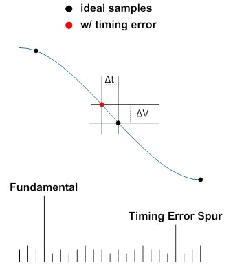
Figure 5: An example timing mismatch waveform and the resulting output spectrum
As an alternative to calibration we can effectively eliminate timing mismatch with a multi-rank Track & Hold (T&H) that utilizes a single sampling circuit operating at the highest frequency, fs. Once the high speed signal is sampled, it is then distributed to multiple lower-speed samplers and quantizers. In this way timing skews between interleaved units are less critical. This is the approach taken with City Semiconductor’s current Gigasample-per-second (GS/s) family of ADCs.
In the below example diagram, only the clock going to the “TH” block is critical. All other clocks are not as critical because they are sampling a signal that is held constant. Additionally, each individual ADC unit only needs to convert at 1/N of the full sampling rate.
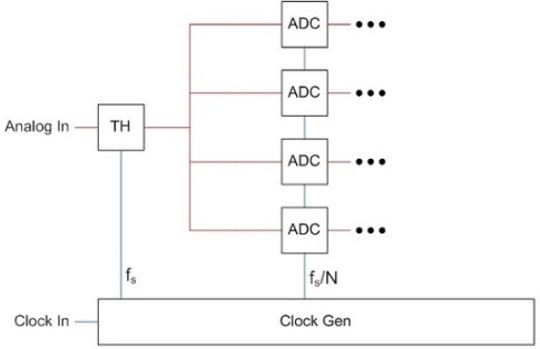
Figure 6: An example of an interleaved ADC with single up-front T&H
This approach is quite effective with a good CMOS process and clock speeds up to 3 GHz. As we move to higher sampling rates a single T&H will suffer from various dynamic effects, and the loading from multiple interleaved quantizers will become prohibitive. At that point the input T&H must also be interleaved, and static timing mismatch corrected by some form of calibration.
One option to calibrate for static timing mismatch is to use an iterative “detect and adjust” approach that senses the voltage errors on a known reference signal caused by timing mismatch, and adjusts a delay line to offset one T&H’s sampling instant with respect to the others until the error is reduced to an acceptable level. The challenge, of course, is injecting this reference signal and measuring it in a repeatable way.

Figure 7: An example of an interleaved ADC with timing calibration
Another option is to use digital post-processing and a mathematical model based on taking the discrete time derivative to estimate the error based on live data. Several recent conference and journal articles describe such a technique. The cost of this approach is increased digital complexity, and perhaps a reduced usable input frequency range.
Note that bandwidth mismatch is a less common effect which can usually be accounted for with good layout practices, so we won’t discuss it here separately. The spur it creates in the output spectrum is in the same location as the spur caused by timing mismatch.
Putting It All Together
The latest 2.5-GSPS ADC family from City Semiconductor includes circuitry for both foreground and background calibration, to provide the most flexible solution for a wide variety of applications. All reference circuitry is provided on-chip.
While we don’t expect more than one form of calibration would be needed for a single application, when working with IP it is important to be able to quickly port the design from one application to the next, in a variety of process nodes. It is also important to understand the various causes and effects of mismatch in interleaved data converter arrays, and choose the right type of calibration for the target application.
About City Semiconductor, Inc.
City Semiconductor is a mixed-signal IC design house providing world-class intellectual property for the highest-speed applications, specializing in data converters (ADC’s and DAC’s) that operate in the Gigahertz range. City Semiconductor also provides custom and semi-custom design and layout services, and supports all aspects of production release for complex system-on-chip ASICs. Their quickly-growing portfolio includes proven designs implemented in nodes ranging from 40nm to 180nm, at popular foundries worldwide.
City Semiconductor is located in San Francisco, California, and can be found at www.citysemi.com
