Kamalpreet Kaur, Nishant Madan, Syed Shakir Iqbal
Freescale Semiconductor India Pvt. Ltd.
Introduction
With prior knowledge of delay characterization for combinational standard cells, where the delay values are dependent on the input slew and the output load, one needs to take in account of the propagation delay in picture. The scenario gets a bit complex when it comes to sequential elements. Modeling setup time, hold time, C-Q delay and various other factors add more complexity to the characterization to sequential elements. This paper discusses the models and methodology that are used commonly for characterizing the timing parameters of various sequential logic cells which are key elements of synchronous design.
Timing Parameters in a Sequential Cell
While the timing parameters of a combinational cell are limited to min and max delays using the input transition, the output load and the timing model of the cell as a set of variables, sequential cells come up with their own set of complex timing checks. These new requirements use the basics of combinational delay characterization along with an event driven (clock signal level change/transition) constraint to model the primary timing checks and parameters required to completely specify a sequential cell in terms of timing. Some of the key parameters that we will discuss in this paper include:
- Setup Time
- Hold Time
- Clock to Out (C-Q) Delay
- Min Pulse Width
Methodology for Finding the Sequential Delays of a Standard Cell
With combinational element concerned only with the propagation delay of the cell, the sequential element are bit more complex in this scenario. With different arcs it is necessary to model setup time, hold time and c-q delay of a flop while modeling it into the library. The number of arcs required to model can vary within the sequential elements. In this paper we will be discussing about the methodology to find the setup time, hold time or C-Q delay of flip-flops and latches. The min pulse width requirements as discussed in the previous section are a derivative of setup and hold time itself and hence will be implicitly covered.
a) Setup Time:
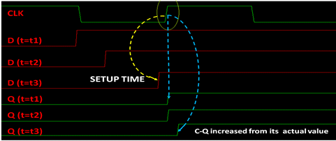
Setup time is a common timing parameter associated with sequential devices. The setup time is used to meet the minimum pulse width requirement for the first (master) latch that makes up a flip flop. More simply, the setup time is the amount of time that an input signal (to the device) must be stable (unchanging) before the clock ticks in order to guarantee minimum pulse width and thus avoid possible meta-stability within the latching loop. The problem comes when one has to find the setup time of a flip flop. This can be easily found out by using spice simulation using below steps:
| Setup time for Flip Flop:
|
Now, one question can arise is why a factor of 10% is taken for calculating the setup time? When we are taking the data transition closer to the active edge of the clock, at the instant when setup time is violated the system goes into a meta-stable state and the output takes longer time to settle down which is the reason for increased C-Q delay.

Figure 1: Setup timing measurement for a positive edge triggered flip-flop.
b) Hold Time:
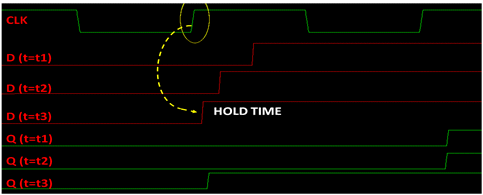
Hold time is also a timing parameter associated with all sequential devices. The Hold time is used to further satisfy the minimum pulse width requirement for the first (Master) latch that makes up a flip flop. The input must not change until enough time has passed after the clock tick to guarantee the master latch is fully disabled. More simply, hold time is the amount of time that an input signal (to a sequential device) must be stable (unchanging) after the clock tick in order to guarantee minimum pulse width and thus avoid possible meta-stability. This can be found out by using spice simulations and following the below mentioned steps:
| Hold Time for Flip Flop:
|

Figure 2: Hold timing measurement for a positive edge triggered flip-flop.
c) Clock to Out (C-Q) Delay:
Clock to out delay is generally considered at infinite setup time. With data making a transition at 10ns before the active clock edge, one can probe the two signals clock and output both at 50% of their voltage levels. The difference between their transitions will give the clock to out or C-Q delay for the flip flop.
d) Min Pulse Width:
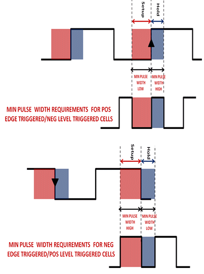
Min pulse width is defined as the minimum permissible pulse width values for both high and low levels below which a given sequential element like flip-flop, latch or SRAM cell will fail to work. It signifies the minimum time these cells will take to function and provide the correct output while being operated. For simulation purposes it is simply another form of representing setup and hold time corresponding to the concerned clock edge and hence can be characterized for different output loads, input slews and triggering events similar to setup and hold time. Figure 3, shows how high and low min pulse width requirements can be modeled based on flop/latch setup and time.

Figure 3: Min Pulse Width and its relationship with setup and hold time.
One key point to note here is that all the SPICE deck analysis involved must be performed for both rise-to-rise and fall-to-fall data transitions for the flip flop as the RC delay parameters and the signal paths vary with respect to the value of data itself.
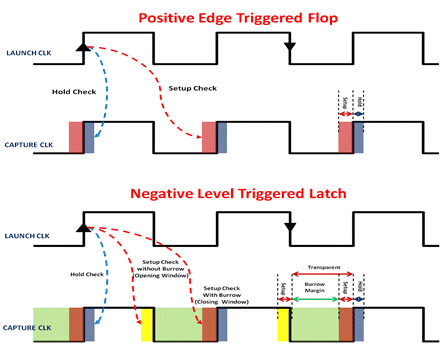
So far all the analysis discussed above has been with a flip-flop or an edge triggered element as a reference. While the definition of setup/hold time and C-Q delay remain same for latches as well, however with the latches being level triggered devices instead of edge triggered, the concept to extract the timing parameters of latch are a bit more tricky. In case of a latch, we need to understand the opening and closing windows for data sampling instead of just a simple edge. Let us consider the timing in a negative level triggered latch as shown in figure 4. The latch will remain transparent in case of a low clock signal while the state will be latched otherwise. Thus, there is an opening window for data sampling when the clock goes low and a closing window when the clock goes high. Now let us add the considerations for setup and hold time into this. Since the circuit elements take a finite time to sample a data in, hence for hold time, the timing requirement is limited with the closing of the latch window (shown in blue in figure 4). This requirement is the same as that in case of a positive edge triggered flip-flop and hence the same setup can be used to measure the hold time. For the case of setup timing, there are two scenarios; setup timing at the opening window and setup timing at the closing window. While the former check is a circuit driven requirement and can be measured by the same method as in the case of positive edge triggered flip-flops, the later check is rather a design driven check used to model time burrowing and is effectively a virtual setup check.

Figure 4: Setup and hold timing for a positive edge triggered flop and negative level triggered latch.
The reason for this check is that unlike a flop, the latch output is not a fixed value during a static clock level. For example, when clock is low, the flop output remains a constant value from the previously captured data, while in case of a negative latch; the output is same as the input data at that instance. Hence, we have a burrow margin which can be given to data path connected at the output of latch, provided we have ensured correct setup timing with the same setup time as at the closing window near the opening edge as shown in figure 3. Hence, to characterize a negative level triggered latch, the characterization methodology is the same as than in case of a positive edge triggered flop and a similar scenario exists for negative edge triggered flop and positive level triggered latch.
Conclusion
This paper elucidates the methodologies followed for setup analysis; hold analysis and setup dependent hold and hold dependent setup analysis. Discussing on the areas of C-Q delays it traverses from setup time to min pulse width checks too for sequential elements flops and latches. This will help persons across industry to understand the sequential cell timing characterization using SPICE and learnt how to use them to get the correct delay estimation.
